Electrical characteristics (continued) – Rainbow Electronics MAX8760 User Manual
Page 7
MAX8760
Dual-Phase, Quick-PWM Controller for AMD
Mobile Turion 64 CPU Core Power Supplies
_______________________________________________________________________________________
7
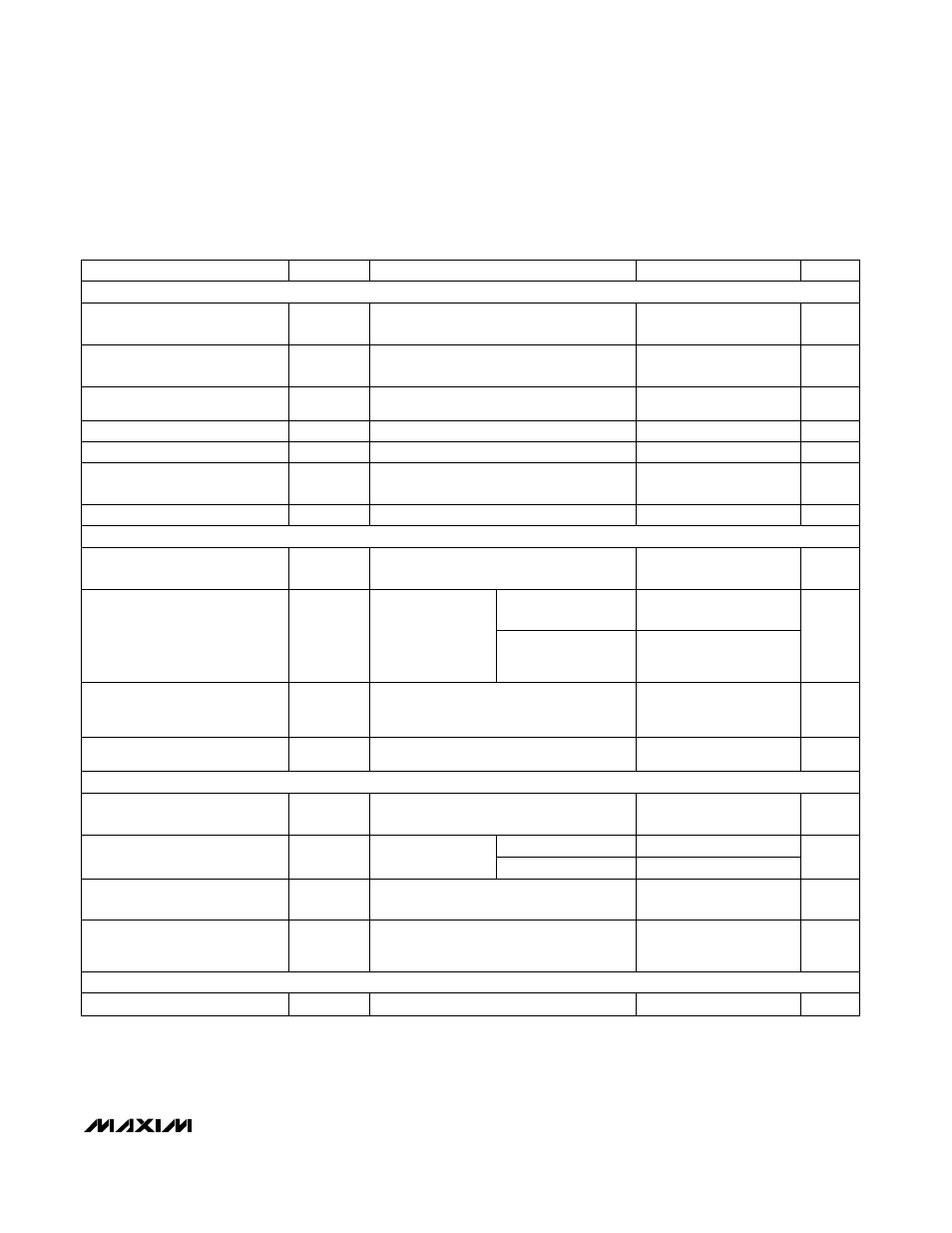
ELECTRICAL CHARACTERISTICS (continued)
(Circuit of Figure 1, V+ = 15V, V
CC
= V
DD
= V
SHDN
= V
SKIP
= V
S0
= V
S1
= 5V, V
FB
= V
CMP
= V
CMN
= V
CSP
= V
CSN
= 1.3V, OFS =
SUS = GNDS = D0–D5 = GND, T
A
= -40°C to +100°C, unless otherwise specified.) (Note 5)
PARAMETER
SYMBOL
CONDITIONS
MIN
MAX
UNITS
BIAS AND REFERENCE
Quiescent Supply Current (V
CC
)
I
CC
Measured at V
CC
, FB forced above the
regulation point, OAIN- = FB, V
OAI N +
= 1.3V
3.2
mA
Quiescent Supply Current (V
DD
)
I
DD
Measured at V
DD
, FB forced above the
regulation point
20
µA
Quiescent Battery Supply Current
(V+)
I
V+
Measured at V+
50
µA
Shutdown Supply Current (V
CC
)
Measured at V
CC
, SHDN = GND
20
µA
Shutdown Supply Current (V
DD
)
Measured at V
DD
, SHDN = GND
20
µA
Shutdown Battery Supply Current
(V+)
Measured at V+, SHDN = GND,
V
CC
= V
DD
= 0V or 5V
20
µA
Reference Voltage
V
REF
V
CC
= 4.5V to 5.5V, I
REF
= 0
1.985
2.015
V
FAULT PROTECTION
Output Undervoltage Protection
Threshold
V
UVP
Measured at FB with respect to unloaded
output voltage
67
73
%
Lower threshold
(undervoltage)
-13
-7
VROK Threshold
Measured at FB
with respect to
unloaded output
voltage
Upper threshold
(overvoltage),
SKIP = V
CC
+7
+13
%
VROK Startup Delay
Measured from the time when FB first
reaches the voltage set by the DAC code
after startup
3
ms
V
CC
Undervoltage Lockout
Threshold
V
UVLO(VCC)
Rising edge, hysteresis = 90mV, PWM
disabled below this level
3.90
4.45
V
CURRENT LIMIT AND BALANCE
Current-Limit Threshold Voltage
(Positive, Default)
V
LIMIT
CMP - CMN, CSP - CSN; ILIM = V
CC
27
33
mV
V
ILIM
= 0.2V
7
13
Current-Limit Threshold Voltage
(Positive, Adjustable)
V
LIMIT
CMP - CMN,
CSP - CSN
V
ILIM
= 1.5V
72
78
mV
Current-Limit Threshold Voltage
(Negative)
V
LIMIT(NEG)
CMP - CMN, CSP - CSN; ILIM = V
CC
,
SKIP = V
CC
-30
-42
mV
Current-Balance Offset
V
OS(IBAL)
(V
CMP
- V
CMN
) - (V
CSP
- V
CSN
); I
CCI
= 0,
-20mV < (V
CMP
- V
CMN
) < 20mV,
1.0V < V
CCI
< 2.0V
-3
+3
mV
GATE DRIVERS
DH_ Gate-Driver On-Resistance
R
ON(DH)
BST_ - LX_ forced to 5V
4.5
Ω