Rainbow Electronics MAX8760 User Manual
Page 36

MAX8760
Dual-Phase, Quick-PWM Controller for AMD
Mobile Turion 64 CPU Core Power Supplies
36
______________________________________________________________________________________
slew the inductor current higher in response to
increased load, and must always be greater than 1. As
h approaches 1, the absolute minimum dropout point,
the inductor current cannot increase as much during
each switching cycle and V
SAG
greatly increases
unless additional output capacitance is used.
A reasonable minimum value for h is 1.5, but adjusting
this up or down allows tradeoffs between V
SAG
, output
capacitance, and minimum operating voltage. For a
given value of h, the minimum operating voltage can be
calculated as:
where
η
OUTPH
is the total number of out-of-phase switch-
ing regulators, V
VPS
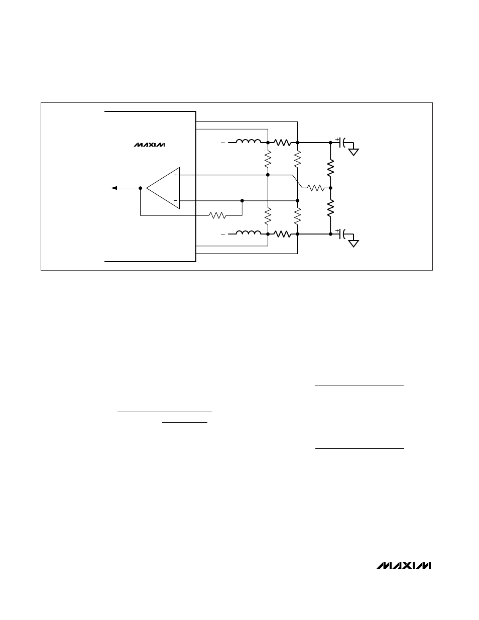
is the voltage-positioning droop,
V
DROP1
and V
DROP2
are the parasitic voltage drops in
the discharge and charge paths (see the On-Time One-
Shot (TON) section), t
OFF(MIN)
is from the Electrical
Characteristics table, and K is taken from Table 6. The
absolute minimum input voltage is calculated with h = 1.
If the calculated V
IN(MIN)
is greater than the required min-
imum input voltage, then reduce the operating frequency
or add output capacitance to obtain an acceptable V
SAG
.
If operation near dropout is anticipated, calculate V
SAG
to
be sure of adequate transient response.
Dropout design example:
V
FB
= 1.4V
K
MIN
= 3µs for f
SW
= 300kHz
t
OFF(MIN)
= 400ns
V
VPS
= 3mV/A
× 30A = 90mV
V
DROP1
= V
DROP2
= 150mV (30A load)
h = 1.5 and
η
OUTPH
= 2
Calculating again with h = 1 gives the absolute limit of
dropout:
Therefore, V
IN
must be greater than 4.1V, even with very
large output capacitance, and a practical input voltage
with reasonable output capacitance would be 5V.
V
x
V
mV
mV
x
s x
s
mV
mV
mV
V
IN MIN
(
)
.
( .
. / .
.
=
+
+
+
=
2
1 4
90
150
1
2
0 4
1 0 3 0
150
150
90
4 07
-
-
-
µ
µ
V
x
V
mV
mV
x
s x
s
mV
mV
mV
V
IN MIN
(
)
.
( .
. / .
.
=
+
+
+
=
2
1 4
90
150
1
2
0 4
1 5 3 0
150
150
90
4 96
-
-
-
µ
µ
V
V
V
V
h x t
K
V
V
V
IN MIN
OUTPH
FB
VPS
DROP
OUTPH
OFF MIN
DROP
DROP
VPS
(
)
(
)
=
+
+
+
η
η
-
-
-
1
2
1
1
MAIN
PHASE
SECOND
PHASE
PC BOARD TRACE
RESISTANCE
ERROR
COMPARATOR
R
F
R
A
R
A
R
B
R
B
OAIN+
OAIN-
FB
PC BOARD TRACE
RESISTANCE
CPU SENSE
POINT
CMP
CMN
CSP
CSN
L1
R
SENSE
R
FBS
L2
R
SENSE
MAX8760
Figure 10. Voltage-Positioning Gain
