Table 6. approximate k-factor errors – Rainbow Electronics MAX8760 User Manual
Page 26
MAX8760
Dual-Phase, Quick-PWM Controller for AMD
Mobile Turion 64 CPU Core Power Supplies
26
______________________________________________________________________________________
On-Time One-Shot (TON)
The core of each phase contains a fast, low-jitter,
adjustable one-shot that sets the high-side MOSFETs
on-time. The one-shot for the main phase varies the on-
time in response to the input and feedback voltages.
The main high-side switch on-time is inversely propor-
tional to the input voltage as measured by the V+ input,
and proportional to the feedback voltage (V
FB
):
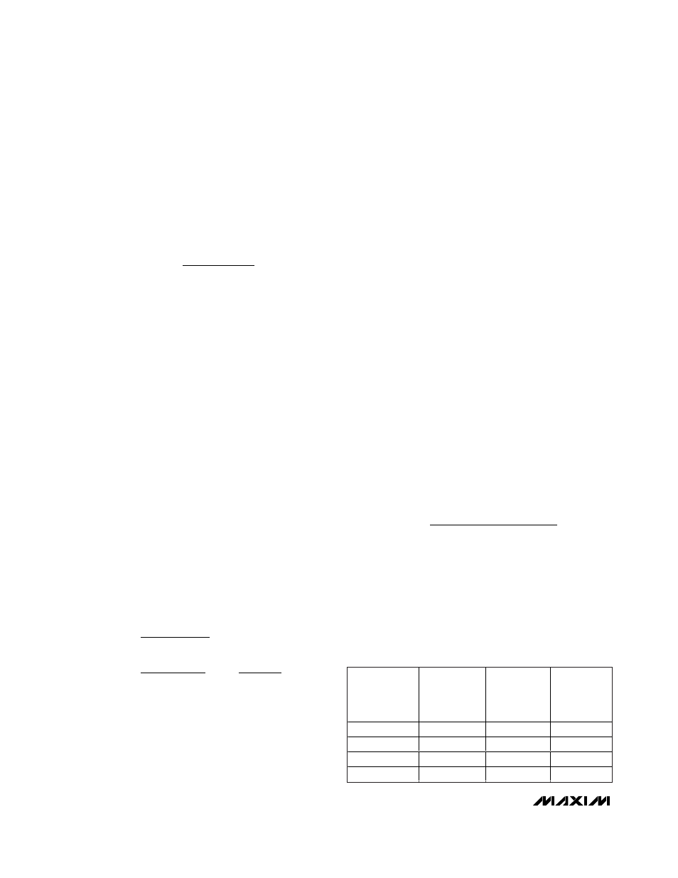
where K is set by the TON pin-strap connection (Table 6)
and 0.075V is an approximation to accommodate the
expected drop across the low-side MOSFET switch.
The one-shot for the secondary phase varies the on-time
in response to the input voltage and the difference
between the main and secondary inductor currents.
Two identical transconductance amplifiers integrate the
difference between the master and slave current-sense
signals. The summed output is internally connected to
CCI, allowing adjustment of the integration time constant
with a compensation network connected between CCI
and FB.
The resulting compensation current and voltage are
determined by the following equations:
where Z
CCI
is the impedance at the CCI output. The
secondary on-time one-shot uses this integrated signal
(V
CCI
) to set the secondary high-side MOSFETs on-time.
When the main and secondary current-sense signals
(V
CM
= V
CMP
- V
CMN
and V
CS
= V
CSP
- V
CSM
) become
unbalanced, the transconductance amplifiers adjust the
secondary on-time, which increases or decreases the
secondary inductor current until the current-sense
signals are properly balanced:
This algorithm results in a nearly constant switching
frequency and balanced inductor currents, despite the
lack of a fixed-frequency clock generator. The benefits of
a constant switching frequency are twofold: first, the
frequency can be selected to avoid noise-sensitive
regions such as the 455kHz IF band; second, the induc-
tor ripple-current operating point remains relatively con-
stant, resulting in easy design methodology and
predictable output-voltage ripple. The on-time one-shots
have good accuracy at the operating points specified in
the Electrical Characteristics table. On-times at operating
points far removed from the conditions specified in the
Electrical Characteristics table can vary over a wider
range. For example, the 300kHz setting typically runs
about 3% slower with inputs much greater than 12V due
to the very short on-times required.
On-times translate only roughly to switching frequencies.
The on-times guaranteed in the Electrical Characteristics
table are influenced by switching delays in the external
high-side MOSFET. Resistive losses, including the induc-
tor, both MOSFETs, output capacitor ESR, and PC board
copper losses in the output and ground tend to raise the
switching frequency at higher output currents. Also, the
dead-time effect increases the effective on-time, reduc-
ing the switching frequency. It occurs only during forced-
PWM operation and dynamic output voltage transitions
when the inductor current reverses at light- or negative-
load currents. With reversed inductor current, the induc-
tor’s EMF causes LX to go high earlier than normal,
extending the on-time by a period equal to the DH-rising
dead time.
For loads above the critical conduction point, where the
dead-time effect is no longer a factor, the actual
switching frequency (per phase) is:
where V
DROP1
is the sum of the parasitic voltage drops in
the inductor discharge path, including synchronous recti-
fier, inductor, and PC board resistances; V
DROP2
is the
sum of the parasitic voltage drops in the inductor charge
path, including high-side switch, inductor, and PC board
resistances; and t
ON
is the on-time as determined above.
f
SW
V
V
t
V
V
V
OUT
DROP
ON
IN
DROP
DROP
=
+
(
)
+
(
)
1
1
2
-
.
.
(
) (
)
(
)
t
K
V
V
V
K
V
V
V
K
I
Z
V
Main on time
Secondary Current
Balance Correction
ON ND
CCI
IN
FB
IN
CCI CCI
IN
2
0 075
0 075
=
+
=
+
+
=
+
−
I
G
V
V
G
V
V
V
V
I
Z
CCI
M
CMP
CMN
M
CSP
CSN
CCI
FB
CCI CCI
=
(
)
(
)
=
+
-
-
-
t
ON MAIN
K V
V
V
FB
IN
(
)
.
=
+
(
)
0 075
Table 6. Approximate K-Factor Errors
TON
CONNECTION
FREQUENCY
SETTING
(kHz)
K-FACTOR
(µs)
MAX
K-FACTOR
ERROR
(%)
V
CC
100
10
±10
Float
200
5
±10
REF
300
3.3
±10
GND
550
1.8
±12.5