Rainbow Electronics MAX8760 User Manual
Page 30
MAX8760
Dual-Phase, Quick-PWM Controller for AMD
Mobile Turion 64 CPU Core Power Supplies
30
______________________________________________________________________________________
Since only the valley current is actively limited, the actu-
al peak current is greater than the current-limit thresh-
old by an amount equal to the inductor ripple current.
Therefore, the exact current-limit characteristic and
maximum load capability are a function of the
current-sense resistance, inductor value, and battery
voltage. When combined with the undervoltage protec-
tion circuit, this current-limit method is effective in
almost every circumstance.
There is also a negative current limit that prevents
excessive reverse inductor currents when V
OUT
is
sinking current. The negative current-limit threshold is
set to approximately 120% of the positive current limit,
and therefore tracks the positive current limit when ILIM
is adjusted. When a phase drops below the negative
current limit, the controller immediately activates an on-
time pulse—DL turns off, and DH turns on—allowing
the inductor current to remain above the negative cur-
rent threshold.
The current-limit threshold is adjusted with an external
resistive voltage-divider at ILIM. The current-limit
threshold voltage adjustment range is from 10mV to
75mV. In the adjustable mode, the current-limit thresh-
old voltage is precisely 1/20 the voltage seen at ILIM.
The threshold defaults to 30mV when ILIM is connected
to V
CC
. The logic threshold for switchover to the 30mV
default value is approximately V
CC
- 1V.
Carefully observe the PC board layout guidelines to
ensure that noise and DC errors do not corrupt the cur-
rent-sense signals seen by the current-sense inputs
(C_P, C_N).
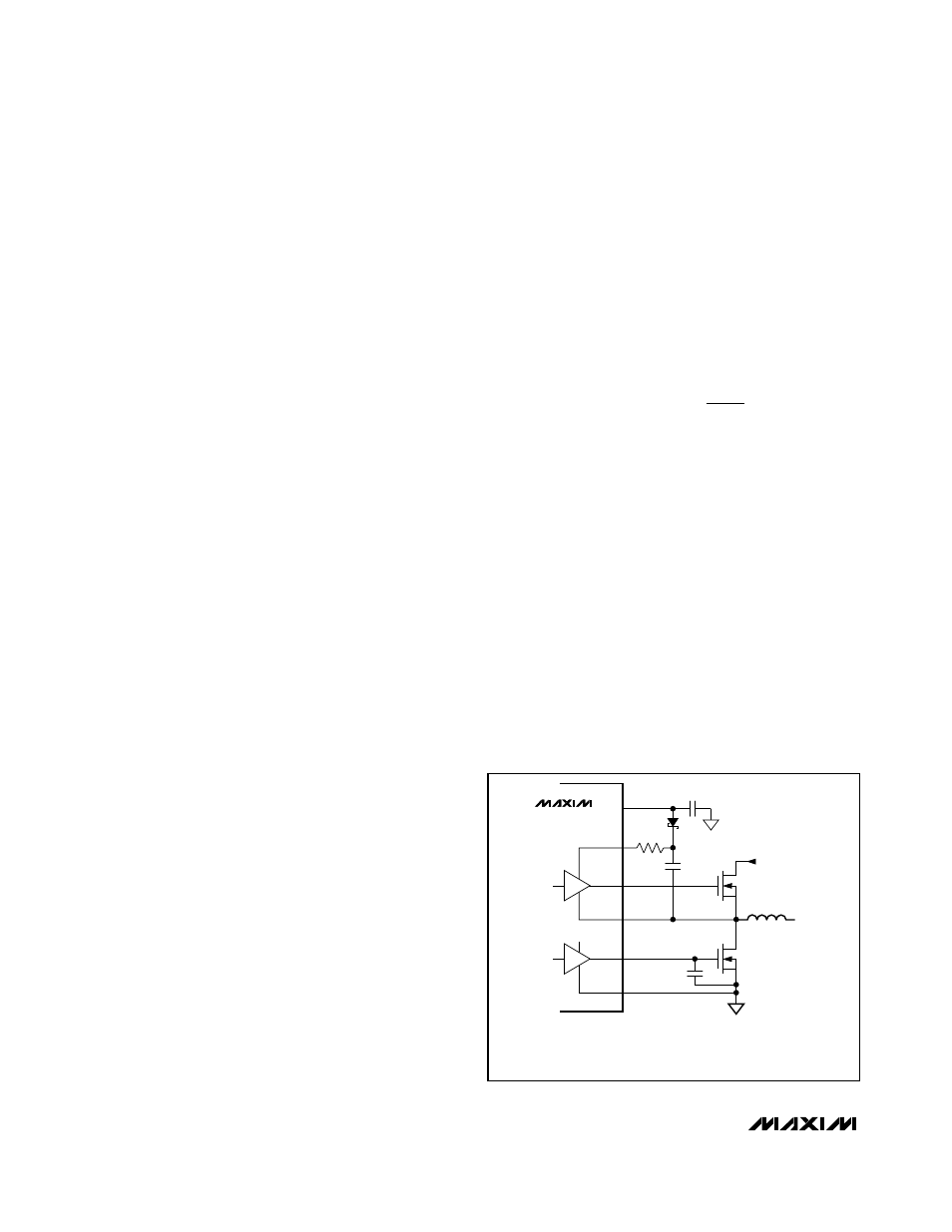
MOSFET Gate Drivers (DH, DL)
The DH and DL drivers are optimized for driving moder-
ately sized, high-side and larger, low-side power
MOSFETs. This is consistent with the low duty factor
seen in the notebook CPU environment, where a large
V
IN
- V
OUT
differential exists. An adaptive dead-time
circuit monitors the DL output and prevents the high-
side FET from turning on until DL is fully off. There must
be a low-resistance, low-inductance path from the DL
driver to the MOSFET gate for the adaptive dead-time
circuit to work properly. Otherwise, the sense circuitry
in the quick-PWM controller interprets the MOSFET gate
as “off” while there is actually charge still left on the
gate. Use very short, wide traces (50 mils to 100 mils
wide if the MOSFET is 1in from the device). The dead
time at the other edge (DH turning off) is determined by
a fixed 35ns internal delay.
The internal pulldown transistor that drives DL low is
robust, with a 0.4
Ω (typ) on-resistance. This helps pre-
vent DL from being pulled up due to capacitive coupling
from the drain to the gate of the low-side MOSFETs when
LX switches from ground to V
IN
. Applications with high
input voltages and long, inductive DL traces may require
additional gate-to-source capacitance to ensure fast-ris-
ing LX edges do not pull up the low-side MOSFET’s gate
voltage, causing shoot-through currents. The capacitive
coupling between LX and DL created by the MOSFET’s
gate-to-drain capacitance (C
RSS
), gate-to-source capac-
itance (C
ISS
- C
RSS
), and additional board parasitics
should not exceed the minimum threshold voltage:
Lot-to-lot variation of the threshold voltage can cause
problems in marginal designs. Typically, adding
4700pF between DL and power ground (C
NL
in
Figure 9), close to the low-side MOSFETs, greatly
reduces coupling. Do not exceed 22nF of total gate
capacitance to prevent excessive turn-off delays.
Alternatively, shoot-through currents may be caused by
a combination of fast high-side MOSFETs and slow low-
side MOSFETs. If the turn-off delay time of the low-side
MOSFET is too long, the high-side MOSFETs can turn
on before the low-side MOSFETs have actually turned
off. Adding a resistor less than 5
Ω in series with BST
slows down the high-side MOSFET turn-on time, elimi-
nating the shoot-through currents without degrading the
turn-off time (R
BST
in Figure 9). Slowing down the high-
side MOSFET also reduces the LX node rise time,
thereby reducing EMI and high-frequency coupling
responsible for switching noise.
Power-On Reset
V
V
C
C
GS TH
IN
RSS
ISS
(
)
>
V
DD
BST
DH
LX
(R
BST
)*
(C
NL
)*
D
BST
C
BST
C
BYP
INPUT
(V
IN
)
N
H
L
V
DD
DL
PGND
N
L
(R
BST
)* OPTIONAL—THE RESISTOR LOWERS EMI BY DECREASING THE SWITCHING
NODE RISE TIME.
(CNL)* OPTIONAL—THE CAPACITOR REDUCES LX TO DL CAPACITIVE COUPLING THAT
CAN CAUSE SHOOT-THROUGH CURRENTS.
Figure 9. Optional Gate-Driver Circuitry