Pin description – Rainbow Electronics MAX8760 User Manual
Page 14
MAX8760
Dual-Phase, Quick-PWM Controller for AMD
Mobile Turion 64 CPU Core Power Supplies
14
______________________________________________________________________________________
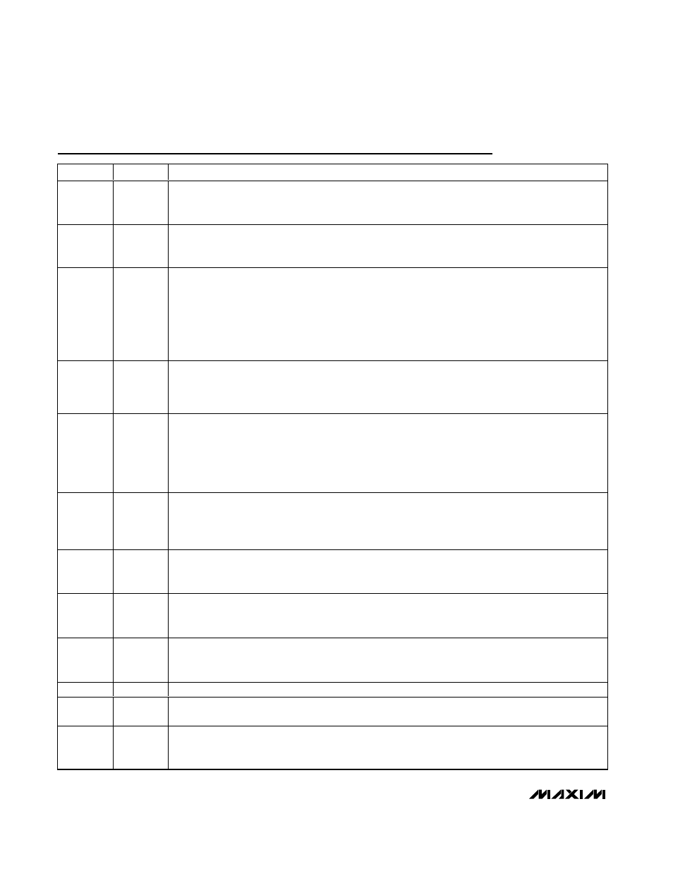
Pin Description
PIN
NAME
FUNCTION
1
TIME
Slew-Rate Adjustment Pin. Connect a resistor from TIME to GND to set the internal slew-rate clock. A
150k
Ω to 15kΩ resistor sets the clock from 100kHz to 1MHz, f
SLEW
= 500kHz x 30k
Ω/R
TIME
. During
startup and shutdown, the internal slew-rate clock operates at 1/4 the programmed rate.
2
TON
On-Time Selection Control Input. This four-level input sets the K-factor value used to determine the DH_
on-time (see the On-Time One-Shot (TON) section): GND = 550kHz, REF = 300kHz, OPEN = 200kHz,
V
CC
= 100kHz
3
SUS
Suspend Input. SUS is a tri-level logic input. When the controller detects on-transition on SUS, the
controller slews the output voltage to the new voltage level determined by SUS, S0, S1, and D0–D5. The
controller blanks VROK during the transition and another 24 R
TIME
clock cycles after the new DAC code
is reached. Connect SUS as follows to select which multiplexer sets the nominal output voltage:
3.3V or V
CC
(high) = Suspend mode; S0, S1 low-range suspend code (Table 5)
REF = Suspend mode; S0, S1 high-range suspend code (Table 5)
GND = Normal operation; D0–D5 VID DAC code (Table 4)
4, 5
S0, S1
Suspend-Mode Voltage-Select Inputs. S0, S1 are four-level digital inputs that select the suspend mode
VID code (Table 5) for the suspend mode multiplexer inputs. If SUS is high, the suspend mode VID code
is delivered to the DAC (see the Internal Multiplexers section), overriding any other voltage setting
(Figure 3).
6
SHDN
S hutd ow n C ontr ol Inp ut. Thi s i np ut cannot w i thstand the b atter y vol tag e. C onnect to V
C C
for nor m al op er ati on.
C onnect to g r ound to p ut the IC i nto i ts 1µA ( typ ) shutd ow n state. D ur i ng the tr ansi ti on fr om nor m al op er ati on
to shutd ow n, the outp ut vol tag e r am p s d ow n at 4 ti m es the outp ut- vol tag e sl ew r ate p r og r am m ed b y the TIM E
p i n. In shutd ow n m od e, D LM and D LS ar e for ced to V
D D
to cl am p the outp ut to g r ound . For ci ng SH DN to 12V
~ 15V d i sab l es b oth over vol tag e p r otecti on and und er vol tag e p r otecti on ci r cui ts, d i sab l es over l ap op er ati on,
and cl ear s the faul t l atch. D o not connect SH DN to > 15V .
7
OFS
Voltage-Divider Input for Offset Control. For 0 < V
OFS
< 0.8V, 0.125 times the voltage at OFS is
subtracted from the output. For 1.2V < V
OFS
< 2V, 0.125 times the difference between REF and OFS is
added to the output. Voltages in the 0.8V < V
OFS
< 1.2V range are undefined. The controller disables the
offset amplifier during suspend mode (SUS = REF or high).
8
REF
2V Reference Output. Bypass to GND with a 0.22µF or greater ceramic capacitor. The reference can
source 100µA for external loads. Loading REF degrades output voltage accuracy according to the REF
load regulation error.
9
ILIM
Current-Limit Adjustment. The current-limit threshold defaults to 30mV if ILIM is connected to V
CC
. In
adjustable mode, the current-limit threshold voltage is precisely 1/20 the voltage seen at ILIM over a
0.2V to 1.5V range. The logic threshold for switchover to the 30mV default value is approximately V
CC
-
1V
10
V
CC
Analog Supply Voltage Input for PWM Core. Connect V
CC
to the system supply voltage (4.5V to 5.5V)
with a series 10
Ω resistor. Bypass to GND with a 1µF or greater ceramic capacitor, as close to the IC as
possible.
11
GND
Analog Ground. Connect the MAX8760’s exposed pad to analog ground.
12
CCV
Voltage Integrator Capacitor Connection. Connect a 47pF to 1000pF (150pF typ) capacitor from CCV to
analog ground (GND) to set the integration time constant.
13
GNDS
Ground Remote-Sense Input. Connect GNDS directly to the CPU ground-sense pin. GNDS internally
connects to an amplifier that adjusts the output voltage, compensating for voltage drops from the
regulator ground to the load ground.