Section 3.3 – Texas Instruments TMS320C6457 User Manual
Page 15

HDS1
HDS2
HCS
HRDY
Internal
HSTRB
Internal
HRDY
www.ti.com
HPI Operation
If the host wants to read data from the DSP internal/external memory, the HPI DMA logic reads the
memory address from HPIAR and retrieves the data from the addressed memory location. When the data
has been placed in HPID, the HPI drives the data onto its HD bus. The HRDY signal informs the host
whether the data on the HD bus is valid (HRDY low) or not valid yet (HRDY high). When the data is valid,
the host latches the data and drives the connected data strobe (HDS1 or HDS2) inactive, which, in turn,
will cause the internal strobe (internal HSTRB) signal to transition from low to high.
If the host wants to write data to the DSP internal/external memory, the operation is similar. After the host
determines that the HPI is ready to latch the data (HRDY is low), it must cause internal HSTRB to
transition from low to high, which causes the data to be latched into HPID. Once the data is in HPID, the
HPI DMA logic reads the memory address from HPIAW and transfers the data from HPID to the
addressed memory location.
3.3
HDS2, HDS1, and HCS: Data Strobing and Chip Selection
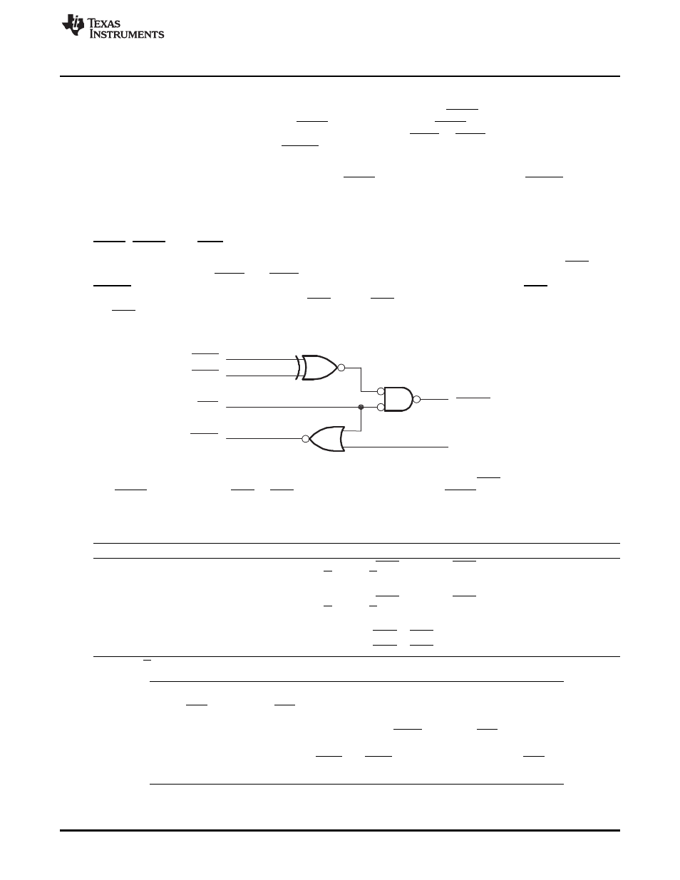
As illustrated in
, the strobing logic is a function of three key inputs: the chip select pin (HCS) and
two data strobe signals (HDS1 and HDS2). The internal strobe signal, which is referred to as internal
HSTRB throughout this document, functions as the actual strobe signal inside the HPI. HCS must be low
(HPI selected) during strobe activity on the HDS pins. If HCS remains high (HPI not selected), activity on
the HDS pins is ignored.
Figure 6. HPI Strobe and Select Logic
Strobe connections between the host and the HPI partially depend on the number and types of strobe pins
available on the host.
describes various options for connecting to the HDS pins. Notice in
that HRDY is also gated by HCS. If HCS goes high (HPI not selected), HRDY goes low, regardless of
whether the current internal transfer is completed in the DSP.
Table 3. Options for Connecting Host and HPI Data Strobe Pins
Available Host Data Strobe Pins
Connections to HPI Data Strobe Pins
Host has separate read and write strobe
Connect one strobe pin to HDS1 and other to HDS2
(1)
. Because such a host might not
pins, both active-low
provide an R/W line, HR/W timings must be satisfied as stated in the device datasheet,
perhaps by using a host address line.
Host has separate read and write strobe
Connect one strobe pin to HDS1 and other to HDS2
(1)
. Because such a host might not
pins, both active-high
provide an R/W line, HR/W timings must be satisfied as stated in the device datasheet,
perhaps by using a host address line.
Host has one active-low strobe pin
Connect the strobe pin to HDS1 or HDS2, and connect the other pin to logic level 1.
Host has one active-high strobe pin
Connect the strobe pin to HDS1 or HDS2, and connect the other pin to logic level 0.
(1)
The HR/W signal could be driven by a host address line in this case.
NOTE:
1. The HCS input and one HDS strobe input can be tied together and driven with a single
strobe signal from the host. This technique selects the HPI and provides the strobe
simultaneously. When using this method, note that HRDY is gated by HCS as previously
described.
2. It is not recommended to tie both HDS1 and HDS2 to static logic levels and use HCS as
a strobe.
15
SPRUGK7A – March 2009 – Revised July 2010
Host Port Interface (HPI)
Copyright © 2009–2010, Texas Instruments Incorporated
