6 chipset support components – Intel SERVER BOARD SDS2 User Manual
Page 32
I/O Subsystem
Intel® Server Board SDS2
Revision 1.2
Order Number: A85874-002
18
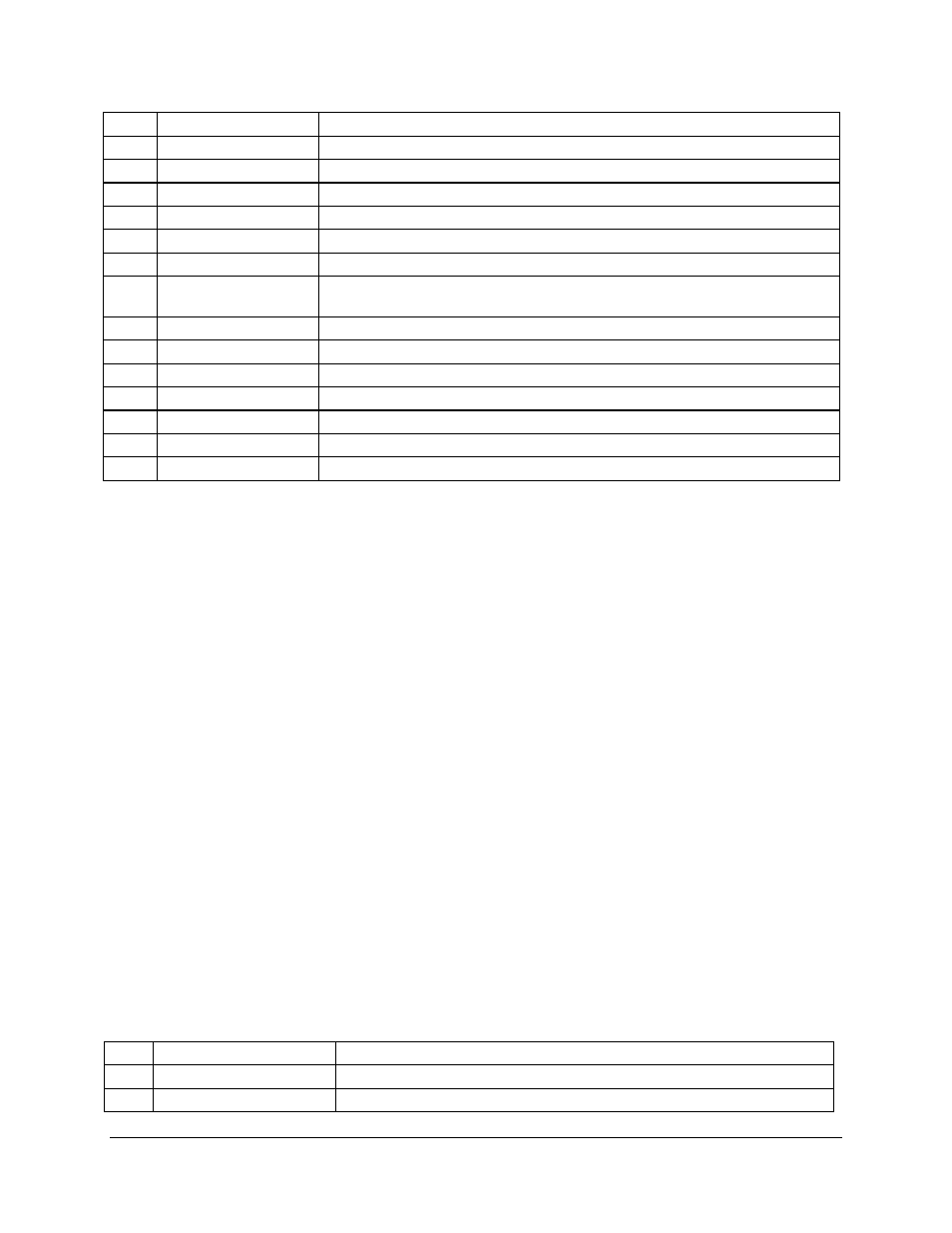
Pad
GPIO Name
Description
Y19
N_NVRAMCLR
Input from jumper to be in BIOS Recovery mode in case of corruption
V17
N_PASSDIS_00
Input from jumper to clear password assignments
U16
N_CMOSCLR_00
Input from jumper to clear setup info in CMOS
T20
N_F3SETUPEN_00
Input from jumper to to be in special test mode (manufacturing only)
T19
N_BMC_SCIN
Input from BMC of SCI event
T18
N_BMCISPMD_00
Input from jumper to to be in special test mode (manufacturing only)
U18
N_FRB3STP_00
Output signal to turn off FRB timer to stop fault conditions (this signal is wire-or
with the 2-pin jumper
Y16
N_SCSI_IDSEL_EN
Output signal to disable onboard SCSI controller
V12
N_LAN2_IDSEL_EN
Output signal to disable onboard NIC2
U12
N_LAN1_IDSEL_EN
Output signal to disable onboard NIC1
V19
CSBPICD0
CSB5 APIC Data Bus 0
W20
CSBPICD1
CSB5 APIC Data Bus 1
Y20
N_ROM_CSN
Output signal for BIOS Chip Select
U19
N_VGA_IDSEL_EN
Output signal to disable onboard Video
4.6 Chipset Support Components
4.6.1
Super I/O
The National Semiconductor PC87417 Super I/O device contains all of the necessary circuitry to
control two serial ports, one parallel port, floppy disk, and PS/2-compatible keyboard and mouse.
The SDS2 Server Board supports the following features:
•
GPIO
•
Two serial ports
•
Floppy
•
Keyboard and mouse through PS/2 connectors
•
Parallel port
•
Real-time clock
•
Wake-up control
4.6.1.1
General Purpose Input and Output - GPIO
The National Semiconductor* PC87417 Super I/O provides number of general-purpose
input/output pins that the SDS2 Server Board utilizes. The following table identifies the pin, the
signal name used in the schematic and a brief description of its usage.
Table 11. Super I/O GPIO Usage Table
Pin #
Signal Name
Description
10
N_BMC_SYSIRQ_00
System Interrupt Controller interrupt from BMC
13
N_SIO_CLK_40M_BMC
40MHz clock output to BMC