Figure 325. halt bus cycle, Table 36. halt bus cycle pin states – Intel 80C188XL User Manual
Page 110
3-29
BUS INTERFACE UNIT
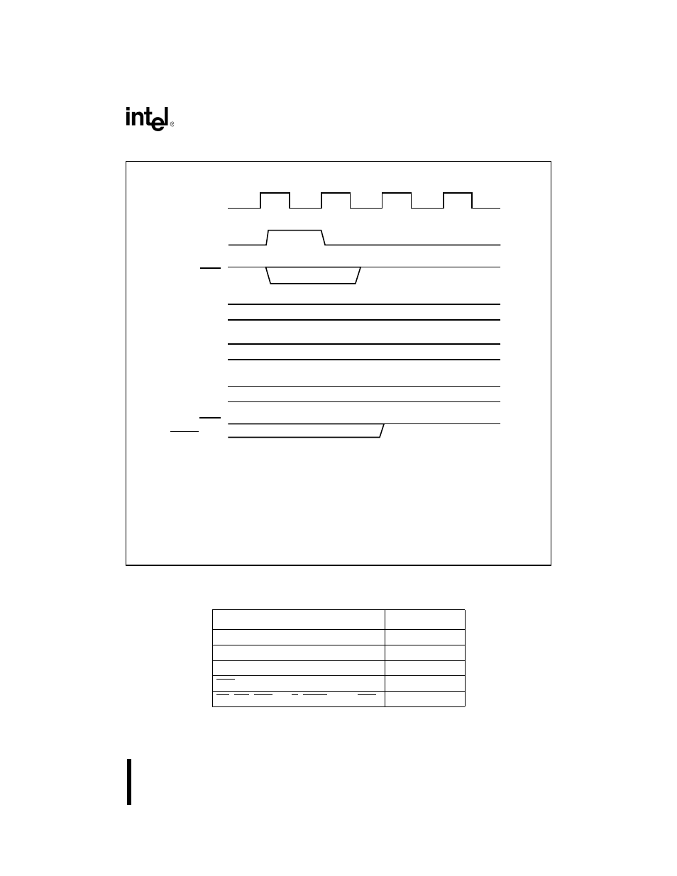
Figure 3-25. HALT Bus Cycle
Table 3-6. HALT Bus Cycle Pin States
Pin(s)
Pin State
AD15:0 (AD7:0 for 8-bit)
Float
A15:8 (8-bit)
Drive Address
A19:16
Drive 8H or Zero
BHE (16-bit)
Drive Last Value
RD, WR, DEN, DT/R, RFSH (8-bit), S2:0
Drive One
011
CLKOUT
ALE
S2:0
AD15:0
[AD7:0]
[A15:8]
A19:16
NOTES:
1. The AD15:0 [AD7:0] bus can be floating, driving a previous write data value,
or driving the next instruction prefetch address value. For an 8-bit device,
A15:8 drives either the previous bus address value or the next instruction
prefetch address value.
2. The A19:16 bus drives either zero (all low) or 8H (all low except A19/S6,
which can be high if the previous bus cycle was a DMA or refresh operation).
T1
TI
TI
BHE
[RFSH = 1]
Note 1
Note 1
Note 2
A1513-0A