Figure 95. timer 0 and timer 1 control registers, Figure 9-5 an – Intel 80C188XL User Manual
Page 236
9-7
TIMER/COUNTER UNIT
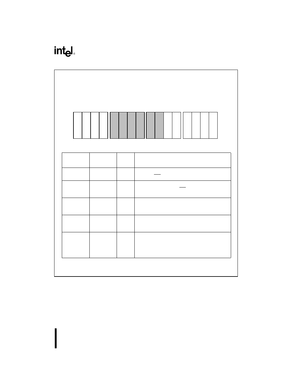
Figure 9-5. Timer 0 and Timer 1 Control Registers
Register Name:
Timer 0 and 1 Control Registers
Register Mnemonic:
T0CON, T1CON
Register Function:
Defines Timer 0 and 1 operation.
Bit
Mnemonic
Bit Name
Reset
State
Function
EN
Enable
0
Set to enable the timer. This bit can be written only
when the INH bit is set.
INH
Inhibit
X
Set to enable writes to the EN bit. Clear to ignore
writes to the EN bit. The INH bit is not stored; it
always reads as zero.
INT
Interrupt
X
Set to generate an interrupt request when the Count
register equals a Maximum Count register. Clear to
disable interrupt requests.
RIU
Register In
Use
X
Indicates which compare register is in use. When set,
the current compare register is Maxcount Compare B;
when clear, it is Maxcount Compare A.
MC
Maximum
Count
X
This bit is set when the counter reaches a maximum
count.
The MC bit must be cleared by writing to the
Timer Control register. This is not done automati-
cally. If MC is clear, the counter has not reached a
maximum count.
NOTE:
Reserved register bits are shown with gray shading. Reserved bits must be written to a
logic zero to ensure compatibility with future Intel products.
15
0
C
O
N
T
A
L
T
E
X
T
R
T
G
M
C
P
R
I
U
I
N
T
I
N
H
E
N
A1297-0A