FUJITSU MHR2030AT User Manual
Page 85
5.2 Logical Interface
C141-E145-02EN
5-11
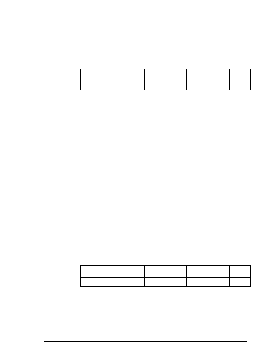
(8) Device/Head register (X’1F6’)
The contents of this register indicate the device and the head number.
When executing INITIALIZE DEVICE PARAMETERS command, the contents
of this register defines “the number of heads minus 1” (a maximum head No.).
Bit 7
Bit 6
Bit 5
Bit 4
Bit 3
Bit 2
Bit 1
Bit 0
X
L
X
DEV
HS3
HS2
HS1
HS0
- Bit 7:
Unused
- Bit 6:
L. 0 for CHS mode and 1 for LBA mode.
- Bit 5:
Unused
- Bit 4:
DEV bit. 0 for the master device and 1 for the slave device.
- Bit 3:
HS3 CHS mode head address 3 (2
3
). bit 27 for LBA mode. Unused
under the LBA mode of the EXT command.
- Bit 2:
HS2 CHS mode head address 2 (2
2
). bit 26 for LBA mode. Unused
under the LBA mode of the EXT command.
- Bit 1:
HS1 CHS mode head address 1 (2
1
). bit 25 for LBA mode. Unused
under the LBA mode of the EXT command.
- Bit 0:
HS0 CHS mode head address 0 (2
0
). bit 24 for LBA mode. Unused
under the LBA mode of the EXT command.
(9) Status register (X’1F7’)
The contents of this register indicate the status of the device. The contents of this
register are updated at the completion of each command. When the BSY bit is
cleared, other bits in this register should be validated within 400 ns. When the
BSY bit is 1, other bits of this register are invalid. When the host system reads
this register while an interrupt is pending, it is considered to be the Interrupt
Acknowledge (the host system acknowledges the interrupt). Any pending
interrupt is cleared (negating INTRQ signal) whenever this register is read.
Bit 7
Bit 6
Bit 5
Bit 4
Bit 3
Bit 2
Bit 1
Bit 0
BSY
DRDY
DF
DSC
DRQ
0
0
ERR