5 pd control instruction (pd) – Yaskawa Ladder Works Programming Manual User Manual
Page 133
7.5 PD CONTROL Instruction (PD)
7-12
7.5 PD CONTROL Instruction (PD)
[Outline]
The PD instruction executes a PD control operation according to the contents of a previously set
parameter table. The input (Input) to the PD operation must be integer or real number data.
Double-length integer data cannot be used. The configurations of the parameter tables for integer
and real number data are different. Operations are performed by processing each parameter as an
integer consisting of the lower-place 16 bits.
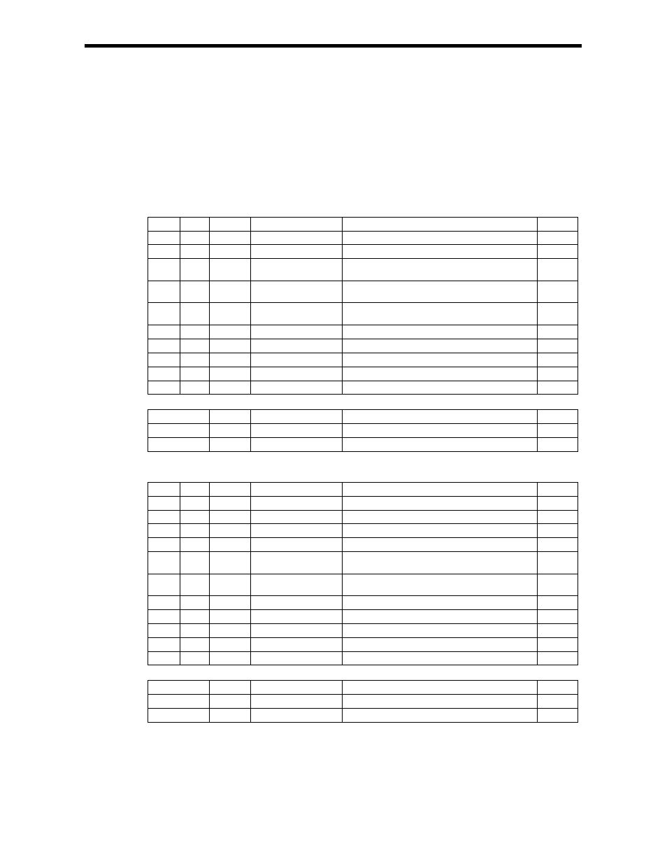
Table of Integer Type PD Instruction Parameters
ADR
Type Symbol
Name
Specification
I/O
0
W
RLY
Relay I/O
Relay input, relay output *
1
IN/OUT
1
W
Kp
P gain
Gain of the P correction (a gain of 1 is set to 100)
IN
2
W
Kd
D gain
Gain of the differentiation circuit input (a gain of
1 is set to 100)
IN
3 W Td1 Divergence
differentiation time
The differentiation time (ms) used in the case of
diverging input.
IN
4 W Td2 Convergence
differentiation time
The differentiation time (ms) used in the case of
converging input.
IN
5
W
UL
Upper PD limit
Upper limit for the P+D correction value
IN
6
W
LL
Lower PD limit
Lower limit for the P+D correction value
IN
7
W
DB
PD output dead band
Width of the dead band for the P+D correction value
IN
8
W
Y
PD output
PD correction output (also output to the A register)
IN
9
W
X
Input value storage
Storage of the present deviation input value
OUT
*
1
: Relay I/O Bit Assignment
BIT
Symbol
Name
Specification
I/O
0 to 7
-
(Reserve)
Reserve relay for input
IN
8 to F
-
(Reserve)
Reserve relay for output
OUT
Table of Real Type PD Instruction Parameters
ADR
Type Symbol
Name
Specification
I/O
0
W
RLY
Relay I/O
Relay input, relay output *
1
IN/OUT
1 W
-
(Reserve) Reserve
register
-
2
F
Kp
P gain
Gain of the P correction
IN
4
F
Kd
D gain
Gain of the differentiation circuit input
IN
6 F Td1 Divergence
differentiation time
The differentiation time (s) used in the case of
diverging input.
IN
8 F Td2 Convergence
differentiation time
The differentiation time (s) used in the case of
converging input.
IN
10
F
UL
Upper PD limit
Upper limit for the P+D correction value
IN
12
F
LL
Lower PD limit
Lower limit for the P+D correction value
IN
14
F
DB
PD output dead band
Width of the dead band for the P+D correction value
IN
16
F
Y
PD output
PD correction output (also output to the A register)
IN
18
F
X
Input value storage
Storage of the present deviation input value
OUT
*
1
: Relay I/O Bit Assignment
BIT
Symbol
Name
Specification
I/O
0 to 7
-
(Reserve)
Reserve relay for input
IN
8 to F
-
(Reserve)
Reserve relay for output
OUT