0 register maps, 1 cio-pdma16 register map – Measurement Computing CIO-PDMAxx User Manual
Page 12
5.0 REGISTER MAPS
5.1 CIO-PDMA16 REGISTER MAP
The CIO-PDMA16 and use eight consecutive I/O addresses in the PC's I/O address
space. The first address, or BASE ADDRESS, is determined by setting a bank of
switches on the board.
The first four addresses access the A & B data ports and DMA and interrupt control
registers of the CIO-PDMA16. The second four registers are directly mapped into the
8254 counter timer chip used for pacing CIO-PDMA16 transfers.
It is easy to read and write to a register. However, register manipulation is best left to
experienced programmers as most CIO-PDMA16 functions are done using Universal
Library.
In summary form, the registers and their function are listed in Table 5-1. Within each
register are eight bits which may constitute a byte of data or eight individual bit
set/read functions.
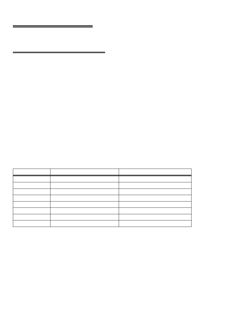
Table 5-1. Register Summary
Counter control
Counter status
BASE +7
Counter 2 data
Counter 2 data
BASE +6
Counter 1 data
Counter 1 data
BASE +5
Counter 0 data
Counter 0 data
BASE +4
Interrupt control, AUX3
Interrupt read back
BASE +3
DMA Control, AUX1 & AUX2
DMA read back
BASE +2
Port B Output
Port B Input
BASE +1
Port A Output
Port A Input
BASE +0
WRITE FUNCTION
READ FUNCTION
ADDRESS
5.1.1 DIGITAL I/O REGISTERS - PORTS A & B
Ports A & B may be written to or read from directly using I/O output or input
commands from any language that has such commands. In this way the
CIO-PDMA16 may be used as a simple digital I/O board.
As a DMA digital I/O board, ports A & B corresponds to the PC data bus. In DMA
word-transfers, port A data is transferred as the least significant byte and port B as the
most significant byte. DMA byte transfers use port A only. Port B cannot be used for
byte transfers under DMA.
8