C.2 power/maintenance board – Comtech EF Data RC-1160 User Manual
Page 62
Theory of Operation
Revision 1
RC-1160 RC-1260 Redundancy Switch Controllers
MN-RC1160RC1260
C-2
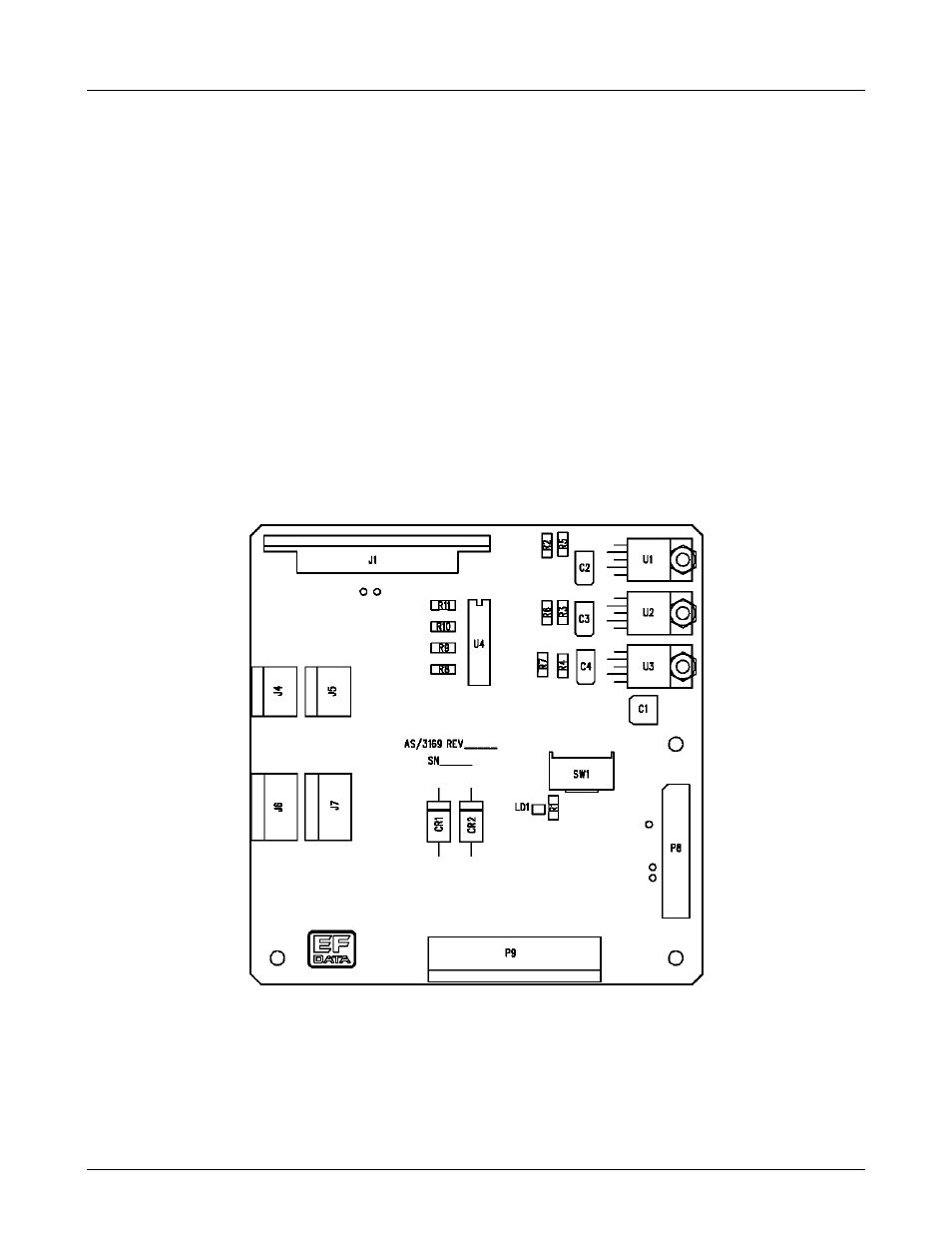
C.2 Power/Maintenance Board
The power/maintenance board (refer to Figure C-1) receives primary and secondary AC power on J4 and J5
pins. This board then routes the primary and secondary AC power to the power supply connectors J6 and J7.
Connectors J4 and J5 are also routed to the waveguide switch PWB on header P9.
The DC power from the power supplies enters on J6 and J7 and is ORed together by CR1 and CR2. The DC
power is then routed to the logic control PWB through header P8.
The DC power is also routed to the maintenance switch, SW1. In maintenance mode, the DC power would be
switched directly to the LNA/LNB outputs on J1.
Commands to position the waveguide switch enter on header P9. The commands are then routed directly to the
LNA/LNB output connector J1.
Position indicator information from the waveguide switch enters on the LNA/LNB connector J1. The
information is then routed to the logic control PWB through header P8.
The common connection to the indicator sensors is tied to ground on pin 17 of J1. This feature makes the active
indicator signal a logic zero. The inactive signals (floating lines) are pulled up to +5 VDC through pull-up
resistors on the logic control PWB.
Figure C-1. Power/Maintenance Board