Table 1 pinout of the headers j202 and tp202, N table 1 – BECKHOFF EL9800 Basisplatine User Manual
Page 13
Product overview
EL9800
11
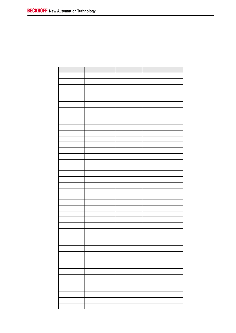
2.2.1 Process data interface dependent pinout of the headers J202 and TP202
The pinout of the headers J202 and TP202 are depending on the choice of the process data interface on
the EL9800 base board. In Table 1 the pinout of these headers are listed for the process interfaces Digital
IO, SPI and the different Microcontroller interfaces.
Table 1 Pinout of the headers J202 and TP202
Pin number
Digital IO
SPI
8/16bit sync./as. µC
1
I/O[0]
GPI[6]
A[0]
2
GND
3
I/O[2]
GPI[4]
A[2]
4
I/O[1]
GPI[5]
A[1]
5
I/O[4]
GPO[6]
A[4]
6
I/O[3]
GPO[7]
A[3]
7
I/O[6]
GPO[4]
A[6]
8
I/O[5]
GPO[5]
A[5]
9
GND
10
I/O[7]
GPI[3]
A[7]
11
I/O[9]
GPI[1]
A[9]
12
I/O[8]
GPI[2]
A[8]
13
I/O[11]
GPO[3]
A[11]
14
I/O[10]
GPI[0]
A[10]
15
I/O[13]
EEPROM Loaded
16
I/O[12]
GPO[2]
A[12]
17
I/O[15]
GPI[11]
CPU_CLK_IN
18
I/O[14]
GPO[1]
A[13]
19
I/O[16]
GPI[7]
D[0]
20
GND
21
I/O[18]
SPI_SEL
D[2]
22
I/O[17]
GPO[8]
D[1]
23
I/O[20]
GPO[11]
D[4]
24
I/O[19]
GPO[10]
D[3]
25
I/O[22]
SPI_INT
D[6]
26
I/O[21]
GPI[8]
D[5]
27
GND
28
I/O[23]
GPI[10]
D[7]
29
I/O[25]
GPO[13]
D[8]
30
I/O[24]
SPI_D_IN
D[8]
31
I/O[27]
GPO[15]
D[11]
32
I/O[26]
SPI_D_OUT
D[10]
33
I/O[29]
GPI[13]
D[13]
34
I/O[28]
GPI[12]
D[12]
35
I/O[31]
GPI[15]
D[15]
36
I/O[30]
GPI[14]
D[14]
37
WD_TRIGGER
SPI_CLK
nCS
38
GND
39
SOF
N.C.
RDnWR/nWR
40
OUT_VALID
N.C.
nTS/nRD
41
SYNC[0]/LATCH[0]