Process data interface for ethercat postage stamps, Figure 6 pinout of the connectors j202 and tp202 – BECKHOFF EL9800 Basisplatine User Manual
Page 12
Product overview
10
EL9800
2.2 Process Data Interface for EtherCAT postage stamps
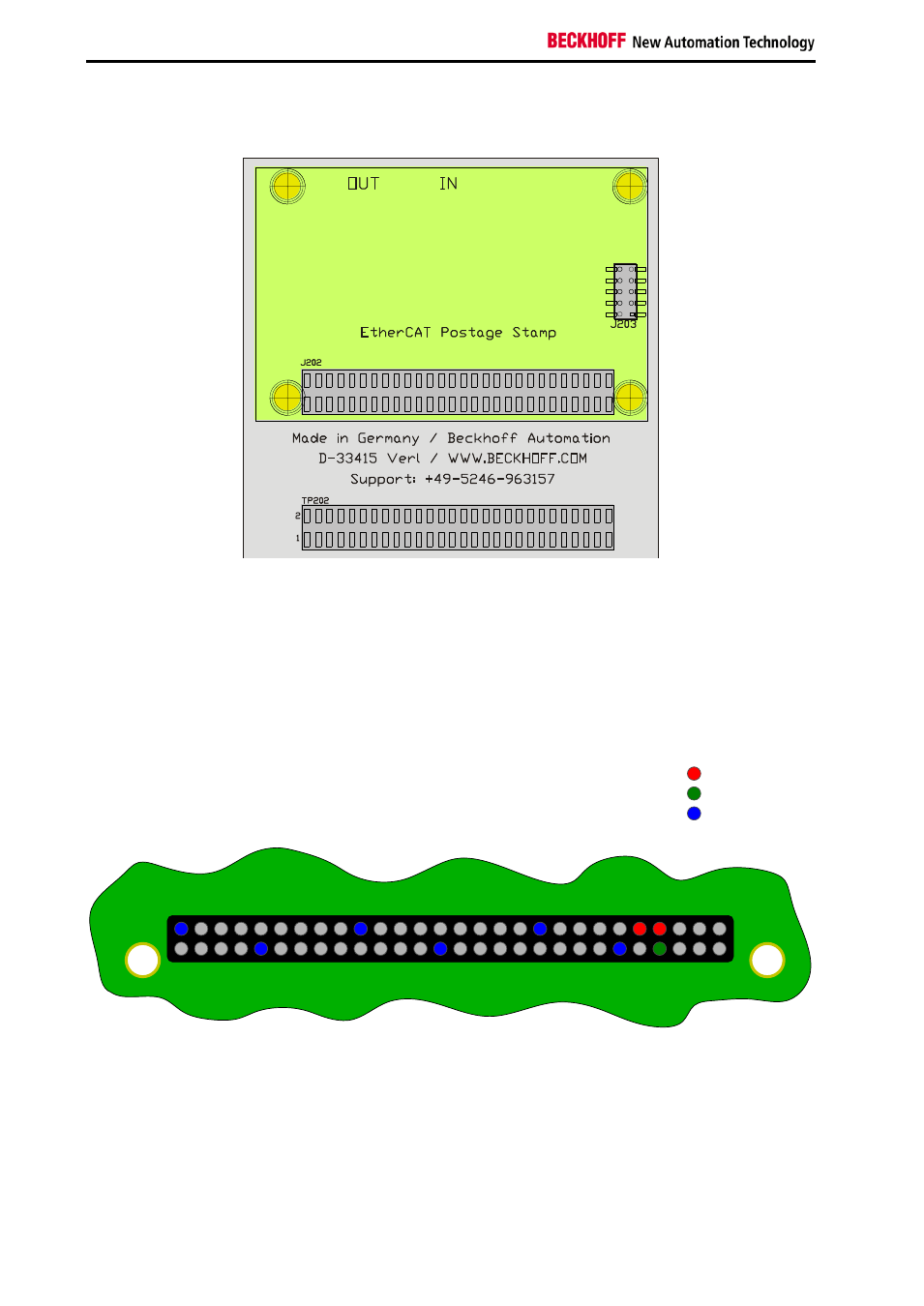
Figure 5 Connection area fort he EtherCAT postage stamp
Within this area all EtherCAT postage stamps are attached to the base board. Communication between
EtherCAT postage stamp and the EL9800 base boards takes place over the connector J202. In case of
FPGA-based EtherCAT Slave Controller boards configuration and debugging of the FPGA is done using
the connector J203. The headers J202 and TP202 pinouts are identical. Therefore all process data sig-
nals of any EtherCAT postage stamp can be measures without delay or be used for external customer
circuitry. The signal definition on the two connectors, despite of the power supply pins, may differ from
EtherCat postage stamp to EhterCAT postage stamp.
2
9
20
27
38
45
48 50
49
VCC (5V)
+3.3V
GND
1
Pin Number
56
55
1
Figure 6 Pinout of the connectors J202 and TP202
Figure 6 shows the pinout of the connectors J202 and TP202 with power in- and outputs signals. Each
EtherCAT postage Stamp supplies its own IO-voltage of 3.3V on the pin 49 on the connectors J202 and
TP202.
Maximal transfer rates between an EtherCAT postage stamp and external circuitry can be achieved when
interfacing with the connector TP202. In this case direct communication between both devices is estab-
lished, bypassing the PDIs bus drivers.