2 memory map, Table 4-4, Memory map – Artesyn COMX-P40x0 ENP2 Installation and Use (August 2014) User Manual
Page 67: Functional description
Functional Description
COMX-P40x0 ENP2 Installation and Use (6806800R95B)
67
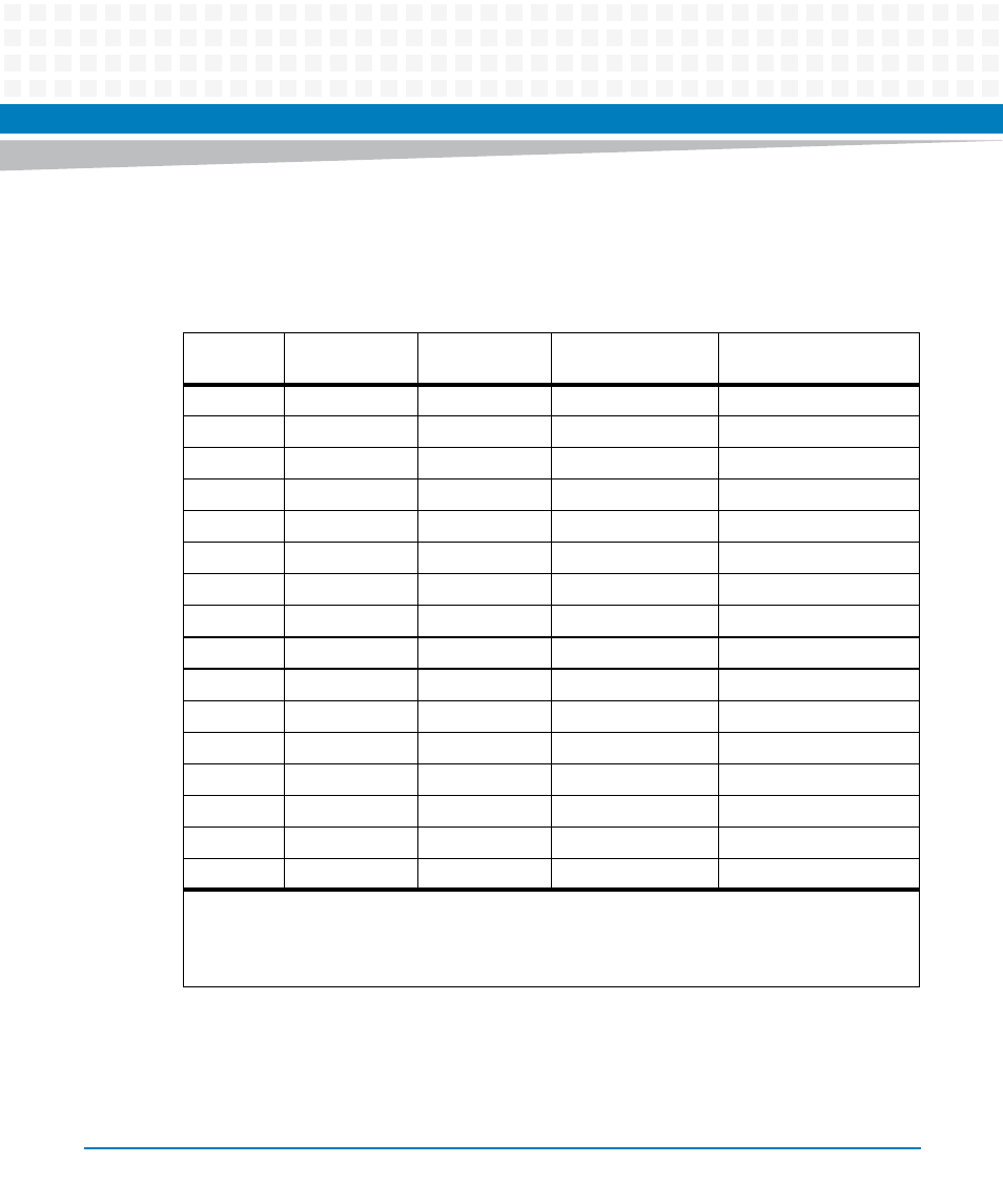
4.8.2
Memory Map
The following table provides the U-boot memory map of the COMX-P40x0 ENP2.
Table 4-4 Memory Map
Address#
32-bit Effective
Base Address
36-bit Physical
Base Address
Size
Description
1.
0000 0000
0 0000 0000
8000 0000 - 2GB
DDR3 Memory, NOTE1
2.
8000 0000
C 0000 0000
2000 0000 - 512MB
PCIE1 MEM
3.
A000 0000
C 2000 0000
2000 0000 - 512MB
PCIE2 MEM, NOTE2
4.
A000 0000
C 2000 0000
1000 0000 - 256MB
RIO1 MEM, NOTE2
5.
B000 0000
C 3000 0000
1000 0000 - 256MB
RIO2 MEM, NOTE2
6.
C000 0000
C 4000 0000
0800 0000 - 512MB
PCIE3 MEM
7.
E000 0000
F E000 0000
1000 0000 - 256MB
LBC NOR FLASH
8.
F000 0000
F F000 0000
0040 0000 - 4MB
DCSR
9.
F400 0000
F F400 0000
0020 0000 - 2MB
BMAN MEM
10.
F420 0000
F F420 0000
0020 0000 - 2MB
QMAN MEM
11.
F800 0000
F F800 0000
0001 0000 - 64KB
PCIE1 IO
12.
F801 0000
F F801 0000
0001 0000 - 64KB
PCIE2 IO
13.
F802 0000
F F802 0000
0001 0000 - 64KB
PCIE3 IO
14.
FFA0 0000
F FFA0 0000
0010 0000 - 1MB
NAND FLASH Buffer
15.
FE00 0000
F FE00 0000
0100 0000 - 16MB
CCSR
16.
FFFF F000
0 FFFF F000
0000 1000 - 4KB
BOOT PAGE
Note1: Only up to 2GB memory is mapped in U-Boot and the other memory is left unmapped and not
used if more than 2GB memory is fitted. More than 2GB can be used in Linux. Up to 4GB has been
verified.
Note2: Address #4 and #5 is used instead of address #3 if RIO is configured