3 nand flash, 6 serdes block, Table 4-2 – Artesyn COMX-P40x0 ENP2 Installation and Use (August 2014) User Manual
Page 62: Nand flash map, Functional description

Functional Description
COMX-P40x0 ENP2 Installation and Use (6806800R95B)
62
4.5.3
NAND FLASH
The NAND FLASH is a Micron MT29F8G08ADADAH4 with a size of 8Gb/1GB. Each page
contains 2112 bytes including 2048 bytes of data and 64 bytes of spare. Each block contains
64 pages including 128KB of data and 4KB of spare. There are a total of 8192 blocks.
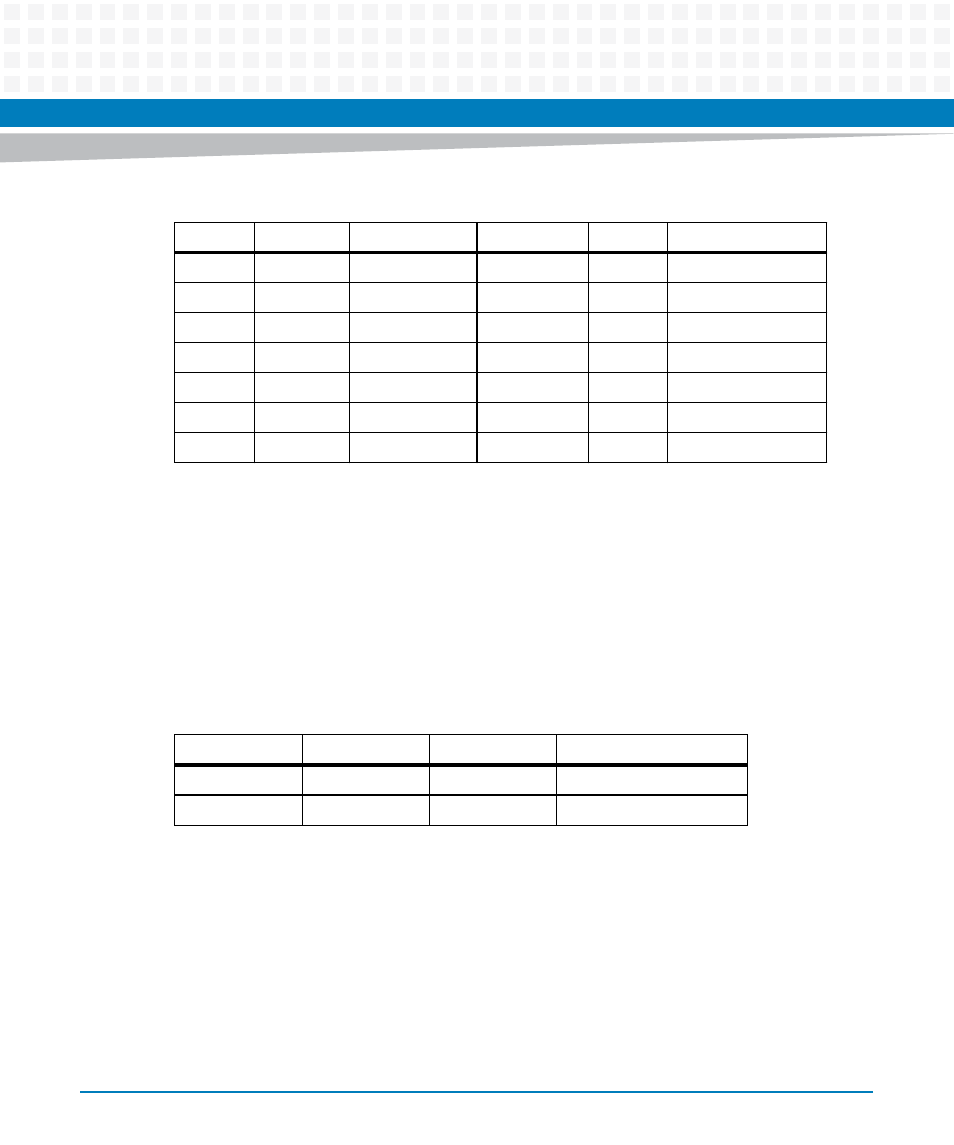
As shipped, the NAND FLASH is only used as NAND FLASH JFFS2 rootfs. The map is described as
below table:
4.6
SERDES Block
The P4040/P4080 CPU provides 3 banks of SERDES with a total of 18 lanes. Bank 1 routes 8
lanes to the COM Express connector as SERDES[0:7]. Bank 2 routes 4 lanes to the COM Express
connector as SERDES[16:19]. Bank 3 also routes 4 lanes to the COM Express connector but is
unused for this module. Bank 1 provides 2 additional SERDES lanes on-board for CPU
debugging through the Aurora interface. See note in the
.
13
3
001A 0000
0020 0000
384KB
Not Used
16
112
0020 0000
00FF FFFF
14 MB
FMAN ucode Image
128
1792
0100 0000
0EFF FFFF
224 MB
RAMDISK Image
1920
120
0F00 0000
0FEF FFFF
15 MB
Kernel Image
2040
3
0FF0 0000
0FF5 FFFF
384 KB
Device Tree Blob
2043
1
0FF6 0000
0FF7 FFFF
128 KB
U-Boot Env Variable
2044
4
0FF8 0000
0FFF FFFF
512 KB
U-Boot Image
Table 4-1 NOR FLASH Map (continued)
Block#
Blocks
Start End
Size
Description
Table 4-2 NAND FLASH Map
Start Address
End Address
Size
Description
0000 0000
00FF FFFF
16 MB
Not Used
0100 0000
3FFF FFFF
1GB - 16MB
NAND FLASH JFFS2 rootfs
