Altera Cyclone III Development Board User Manual
Page 46
2–36
Chapter 2: Board Components
General User Interfaces
Cyclone III 3C120 Development Board Reference Manual
© March 2009 Altera Corporation
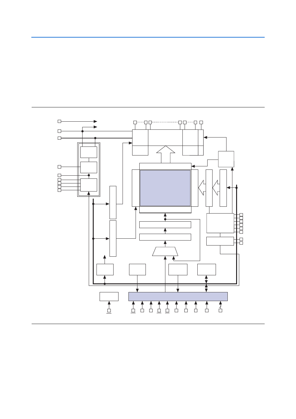
is an excerpt from the OPTREX data sheet showing the control chip in the
LCD module. The control chip is from New Japan Radio Corporation (part number
NJU6676), and
illustrates the functional block diagram of the display
driver.
f
For more information, contact Optrex American at
ew Japan
Radio at
.
Figure 2–9. Graphics LCD Functional Block Diagram of Display Driver
Segment Drivers
Common
Drivers
Shift
Register
Shift
Register
Common
Drivers
Display Data RAM
65 X 132 = 8,580-bit
Display Data Latch
Lo
w
Address Deocder
Line Address Deocder
Column Address Decoder
Vss
VDD
Oscillator
Bus Holder
Busy Flag
Instruction
Decoder
Status
Voltage
Followers
Voltage
Regulator
Voltage
Converter
Multiplexer
Line Co
u
nter
Initial Displa
y Line
Common Direction
P
age Address Register
Column Address Counter
Column Address Register
MPU Interface
Reset
Common
Timing
Display Timing
VR
C1+/C1-
C2+/C2-
C3-
Vss2
Vout
V1 to V6
Internal
Power
Circuits
C0 - - - C21
C63 - - - C32
MS
S0 - - - S131
FR
FRS
CL
CLS
DOF
OSC1
OSC2
D5 to D0
P/S
D6
(SCL)
D7
(SI)
C86
A0
CS2
CS1
WR
Status
Internal Bus Line
RD
RES
COMM