Altera Signal Integrity Development Kit, Stratix V GX Edition User Manual
Page 18
4–6
Chapter 4: Development Board Setup
Factory Default Switch Settings
Transceiver Signal Integrity Development Kit
July 2012
Altera Corporation
Stratix V GX Edition User Guide
8. Set jumper blocks (J26, J28) to match
.
1
For more information about the FPGA board settings, refer to the
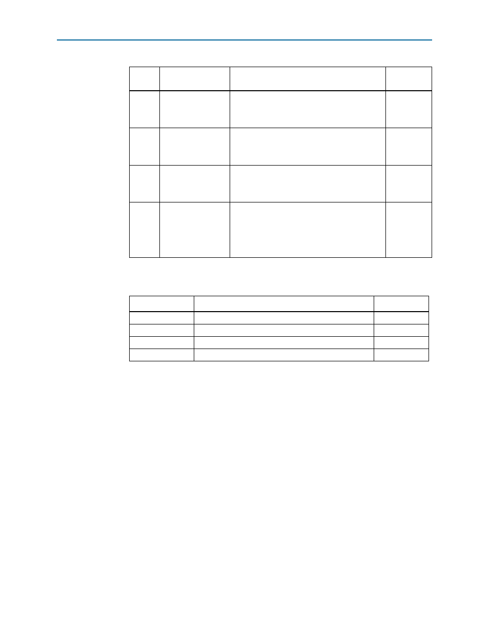
3
MSEL2
Switch 3 has the following options:
■
Logic 0.
■
Logic 1.
1
4
MSEL3
Switch 4 has the following options:
■
Logic 0.
■
Logic 1.
0
5
MSEL4
Switch 5 has the following options:
■
Logic 0.
■
Logic 1.
1
6
MAX BYPASS
Switch 6 has the following options:
■
Logic 0. Includes the MAX II device in the JTAG
chain.
■
Logic 1. Removes the MAX II device in the
JTAG chain.
0
Table 4–8. Jumper Settings
Board Reference
Description
Shunt Position
J26
Fan select — Pins 1-2 select auto operation.
Installed
J26
Fan select — Pins 2-3 select fan on.
Not installed
J28
PGMSEL (logic 1) — Pins 1-2 select user-defined image.
Not Installed
J28
PGMSEL (logic 0) — Pins 2-3 select factory image.
Installed
Table 4–7. S7 Dip Switch Settings (Part 2 of 2)
Switch
Board
Label
Function
Default
Position