Table 4–6 – Altera Signal Integrity Development Kit, Stratix V GX Edition User Manual
Page 17
Chapter 4: Development Board Setup
4–5
Factory Default Switch Settings
July 2012
Altera Corporation
Transceiver Signal Integrity Development Kit
Stratix V GX Edition User Guide
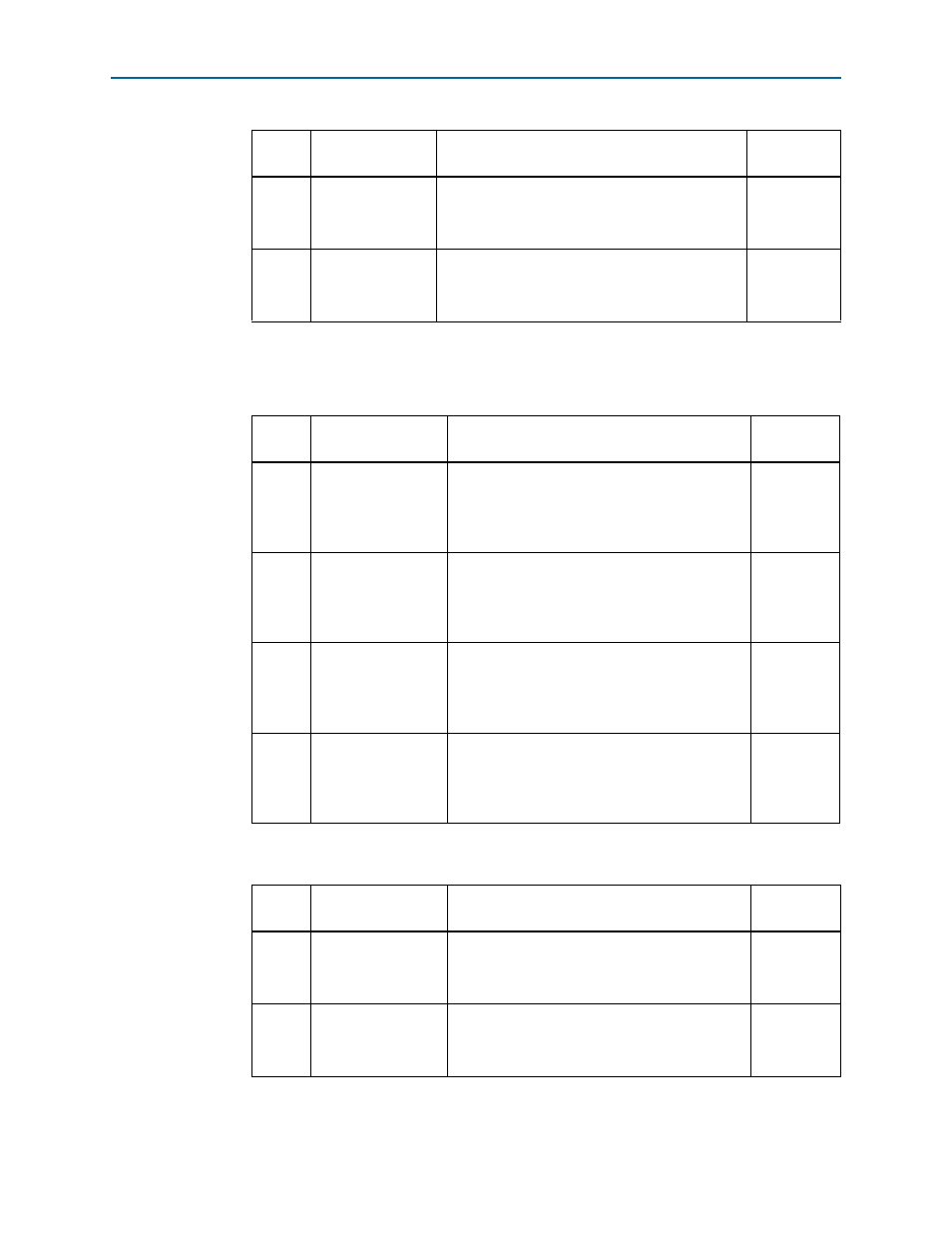
6. For power sequencing, set DIP switch bank (SW7) to match
. (For the other power sequence settings, see
.)
7. Set DIP switch bank (S7) to match
.
3
REFCLK_SEL_U34
Switch 3 has the following options:
■
When set at OSC, enables oscillator input.
■
When set at SMA, enables SMA input.
OSC
4
REFCLK_SEL_U35
Switch 4 has the following options:
■
When set at OSC, enables oscillator input.
■
When set at SMA, enables SMA input.
OSC
Table 4–6. SW7 Dip Switch Settings
Switch
Board
Label
Function
Default
Position
1
SW7-1 2p5V
Switch 1 has the following power sequencing
options:
■
2p5V is enabled.
■
2p5V is disabled.
ENABLED
2
SW7-2 VCCR_GTB
Switch 2 has the following power sequencing
options:
■
VCCR_GTB is enabled.
■
VCCR_GTB is disabled.
ENABLED
3
SW7-3 VCCT_GTB
Switch 3 has the following power sequencing
options:
■
VCCT_GTB is enabled.
■
VCCT_GTB is disabled.
ENABLED
4
SW7-4 VCCL_GTB
Switch 4 has the following power sequencing
options:
■
VCCL_GTB is enabled.
■
VCCL_GTB is disabled.
ENABLED
Table 4–7. S7 Dip Switch Settings (Part 1 of 2)
Switch
Board
Label
Function
Default
Position
1
MSEL0
Switch 1 has the following options:
■
Logic 0.
■
Logic 1.
0
2
MSEL1
Switch 2 has the following options:
■
Logic 0.
■
Logic 1.
0
Table 4–5. SW6 Dip Switch Settings (Part 2 of 2)
Switch
Board
Label
Function
Default
Position