Altera Cyclone V SoC User Manual
Page 40
A–2
Appendix A: Programming Flash Memory
CFI Flash Memory
Cyclone V SoC Development Kit
November 2013
Altera Corporation
User Guide
■
Program the CFI flash memory devices connected to the CPLD I/O pins.
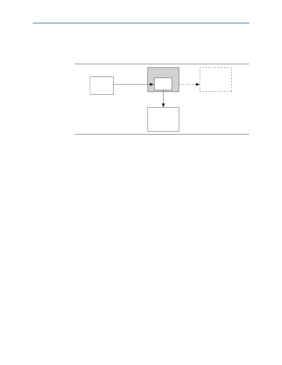
shows an Altera CPLD configured as a bridge to program the CFI flash
memory device through the JTAG interface.
Perform the following steps to program a user design to the flash device in the
Quartus II Programmer:
1
The following flash writing procedure blinks the SEL 2, 1, and 0 LEDs and does not
support the Power Monitor, Clock Control, or other logic functions.
1. On the Tools menu in the Quartus II software, click Programmer.
2. In the Programmer window, click Auto-Detect.
1
If you do not see USB Blaster or the board's embedded USB Blaster II listed
next to Hardware Setup, refer to the
“Installing the USB-Blaster II Driver”
3. Click Add File and open
dir>\kits\cycloneVSX_5csxfc6df31_soc\factory_recovery\max2_PFL_writer.po
f.
4. Turn on the Program/Configure option for the .pof file.
5. Click Start to download the selected configuration file to the MAX V CPLD.
Configuration is complete when the progress bar reaches 100%
6. Click Auto Detect and a flash device should show up attached to the MAX V in
the main window.
7. Double-click the graphic of the flash device in the device chain pane to display the
Device’s Properties
dialog box.
8. Select the flash image .pof file generated from the Quartus II Convert
Programming Files
dialog box. The default file name is output_file.pof.
9. After the flash image .pof is attached in the Quartus II Programmer, turn on
Page_1
and Option Bits. (Page_0 is reserved for the GSRD factory design.)
10. Click Start.
Figure A–1. Programming the CFI Flash Memory With the JTAG Interface
MAX II CPLD
CFI Flash
Memory
Altera
FPGA
Configuration Data
Common
Flash
Interface
PFL
Quartus II
Software
via JTAG
Altera FPGA Not Used
for Flash Programming