A. programming flash memory, Cfi flash memory, Cfi flash memory map – Altera Cyclone V SoC User Manual
Page 39: Appendix a. programming flash memory, Appendix a, programming flash memory

November 2013
Altera Corporation
Cyclone V SoC Development Kit
User Guide
A. Programming Flash Memory
This appendix describes programming information for the following memory
devices:
■
Common flash interface (CFI) flash memory
■
Quad serial peripheral interface (quad SPI) flash memory
■
SD card flash memory
The Cyclone V development board’s flash memory ships preconfigured with the
parallel flash loader (PFL) option bits to support FPGA designs to be written to any of
the three locations as shown in
. The PFL is disabled by default. Set SW2.3 to
ON to enable FPGA programming from CFI flash memory on power up.
1
There are several other factory software files written to flash memory to support the
Board Update Portal. These software files were created using the Nios II EDS, just as
the hardware design was created using the Quartus II software.
CFI Flash Memory
CFI Flash Memory Map
shows the default memory contents of the 512 Mb CFI flash device.
c
Altera recommends that you do not overwrite the factory hardware images unless
you are an expert with Altera tools. If you unintentionally overwrite the factory
hardware or factory software image, refer to
“Restoring the CFI Flash Device to the
Programming CFI Flash Using the Quartus II Programmer
You can use the JTAG interface in Altera CPLDs to indirectly program the flash
memory device. The Altera CPLD JTAG block interfaces directly with the logic array
in a special JTAG mode. This mode brings the JTAG chain through the logic array
instead of the Altera CPLD boundary-scan cells (BSC). The PFL megafunction
provides JTAG interface logic to do the following:
■
Convert the JTAG stream provided by the Quartus II software.
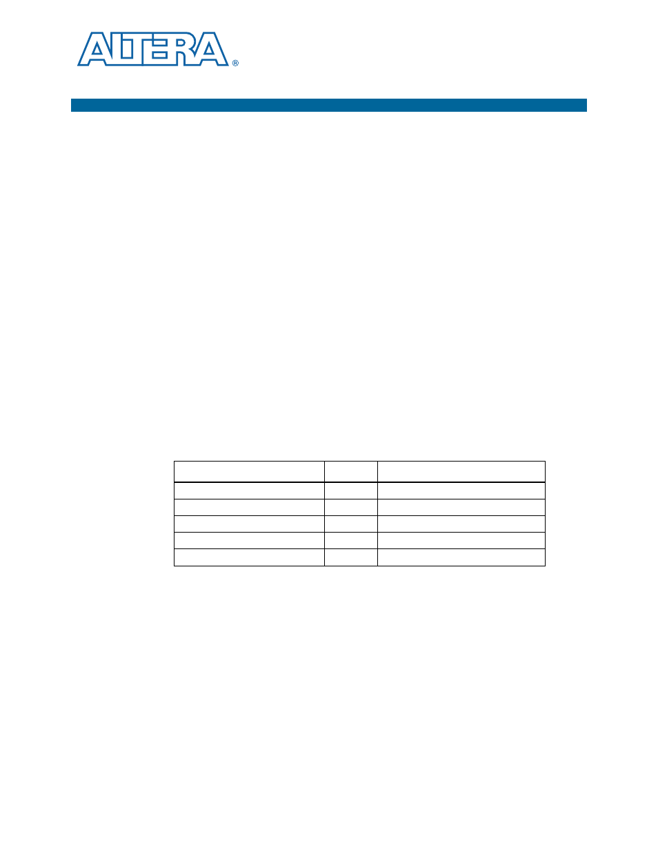
Table A–1. Byte Address Flash Memory Map
Block Description
KB Size
Address Range
Unused
44711
0x0145.635C - 03FF.FFFF
User hardware 2
6872
0x00DA.0000 - 0145.635B
User hardware 1
6872
0x006E.0000 - 00D9.635B
Factory hardware
6872
0x0002.0000 - 006D.635B
PFL option bits
32
0x0001.8000 - 0001.8080
