Static switch, Reserve mo de invert er mo de – OPTI-UPS DS160KD33 User Manual
Page 14
1-10
F
I
L
TER
F
I
L
TER
TO
LO
A
D
TO
LO
A
D
The inverter is composed of IGBT, inductor, capacitor, snubber, control circuitry and
protection circuitry. It can convert the DC power from the DC bus to AC power
supply to the output load. Our UPS use IGBT technology which can switched to
frequency beyond audible range, therefore no audible noise.
Our UPS use voltage regulation circuitry to limit the voltage variation within 1%.
Also special compensation circuitry is added to eliminate the output distortion. Every
component is oversized to accept the wide DC input range (from 285 to 420VDC), so
that the output waveform remains sinusoidal throughout the range. With the aid of
dynamic feedback loop the inverter will keep a sine waveform even under non-linear
load.
We use independent inverter for each phase. Although it is more expensive, each
inverter has its independent feedback, so that the voltage is unaffected when load is
added to the adjacent phase, that is excellent voltage regulation under 100%
unbalanced load.
The IGBT is operated in its optimal condition to obtain best efficiency, so as to
minimize the electricity cost of the user.
Usually, the most frequent failure of UPS happens at the inverter, therefore we added
redundant protection circuitry to protect the inverter, strong snubber is added to
suppress the spikes and noise, use over sized and high quality components, add
semi-conductor fuse and good ventilation etc. Every step aims at a rugged, reliable
and high efficient inverter. At the same time, the inverter can sustain overload and
high peak current drawn by the load. And the MTBF must be long than one expects.
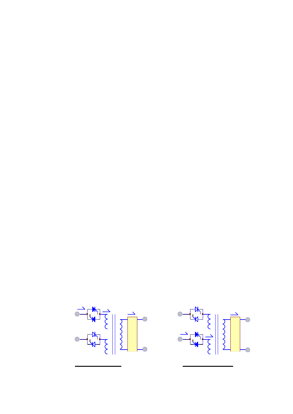
1.5. Static Switch
RESERVE
INVERTER
RESERVE
INVERTER
RESERVE MO DE
INVERT ER MO DE