Opus card – ddr-2 interface, Reference manual – Digilent DDR-2 Opus Card User Manual
Page 17
Opus Card – DDR-2 Interface
Reference Manual
12/03/2010 07:35 AM
17
Copyright © 2009-2010 by CML
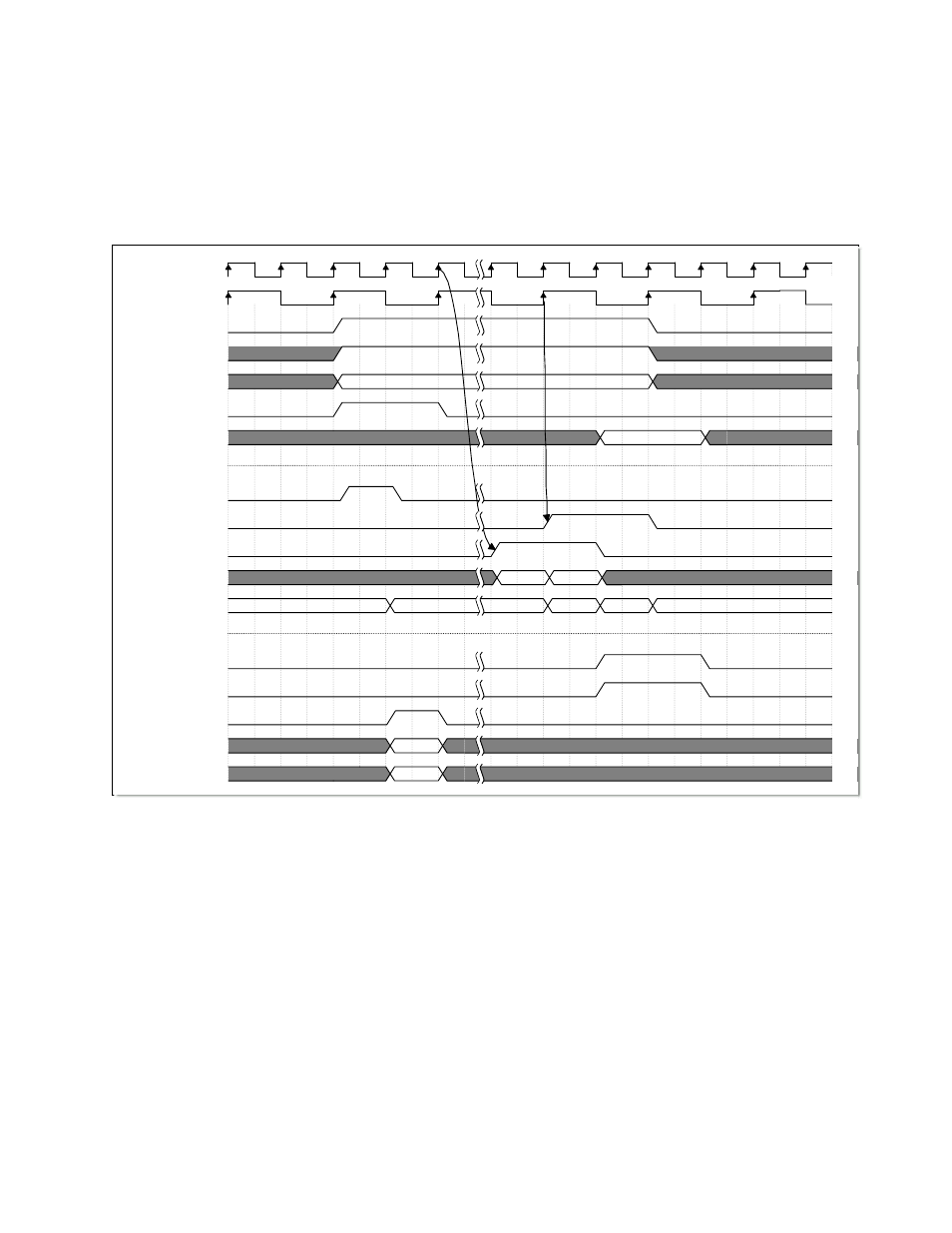
3.3.2 Non-burst, 32-bit Memory Read not Clock-Aligned
The timing diagram below is for a non-burst, 32-bit memory read where Rd_Data_Valid does
not align with the rising edge of Bus2IP_Clk.
1
2
3
4
5
6
7
8
9
10
11
12
Read
Address
Word1
Word2
32-bit Data
Address
Idle
Wait_RdValid
Idle
Wait_RdValid
Rd_Ack1
Rd_Ack2
Signals below are from write_ctrl
TimeGen
DDR2_Clk
Bus2IP_Clk
Bus2IP_CS
Bus2IP_RNW
Bus2IP_Addr
Bus2IP_RdReq
IP2Bus_Data
Rd_Send_Cmd
Rd_Send_Ack
Rd_Data_Valid
Rd_Data_FIFO_Out
State
IP2Bus_AddrAck
IP2Bus_RdAck
App_AF_WREn
App_AF_Cmd
App_AF_Addr
See also other documents in the category Digilent Hardware:
- 410-282P-KIT (4 pages)
- 410-279P-KIT (26 pages)
- 410-258P-KIT (16 pages)
- 410-138P-KIT (28 pages)
- 410-178P-KIT (22 pages)
- 410-292P-KIT (29 pages)
- 410-274P-KIT (29 pages)
- 410-182P-KIT (22 pages)
- 410-134P-KIT (17 pages)
- 410-183P-KIT (19 pages)
- 410-155P-KIT (12 pages)
- 6015-410-001P-KIT (26 pages)
- 410-087P-KIT (164 pages)
- 410-146P-KIT (4 pages)
- 6003-410-000P-KIT (138 pages)
- XUPV2P (23 pages)
- 410-047-C2P-KIT (3 pages)
- WaveForms (85 pages)
- 410-297P-KIT (25 pages)
- 410-295P-KIT (37 pages)
- 410-296P-KIT (23 pages)
- 410-209P-KIT REV.D (16 pages)
- 410-209P-KIT REV.C (17 pages)
- 410-254P-KIT (17 pages)
- 410-280P-KIT (9 pages)
- 410-202P-KIT (20 pages)
- 410-273P-KIT (24 pages)
- 410-269P-KIT (11 pages)
- 410-216P-KIT (15 pages)
- 410-231P-KIT (4 pages)
- 410-211P-KIT (10 pages)
- 410-262P-KIT (8 pages)
- 410-229P (7 pages)
- 410-242P-KIT (4 pages)
- 6021-210-000P-KIT (27 pages)
- 410-185P-KIT (21 pages)
- 6032-410-000P-BOARD (4 pages)
- 410-174P (17 pages)
- 410-145P (6 pages)
- 210-264P-BOARD (3 pages)
- 6003-210-012P (27 pages)
- 410-236P-BOARD (2 pages)
- 410-163P (1 page)
- 410-097P-KIT (2 pages)
- 410-255P-KIT (1 page)