2 power supplies, Power supplies, 2power supplies – Digilent 6015-410-001P-KIT User Manual
Page 5
NetFPGA-1G-CML™ Board Reference Manual
programs the FPGA directly with a special purpose BPI flash interface. It will then transfer the .mcs bitstream to the
flash through that interface. This process is fully automated by the iMPACT program, so a designer only needs to
be concerned with the creation of the .mcs file using Xilinx’s design software.
More details on configuring the XC7K325T FPGA via the on board BPI (using Master BPI mode), via the PIC USB-
HOST (using Slave Serial mode), and via the JTAG mode can be found in the Xilinx 7 Series FPGAs Configuration
User Guide (UG470).
2
Power Supplies
The NetFPGA-1G requires a 12V, 5A, or greater power source. Power is supplied via the J17 Molex connector at the
rear of the PCB, as is often done with high performance PC graphics cards. No power is supplied via the PCIe
motherboard bus connector.
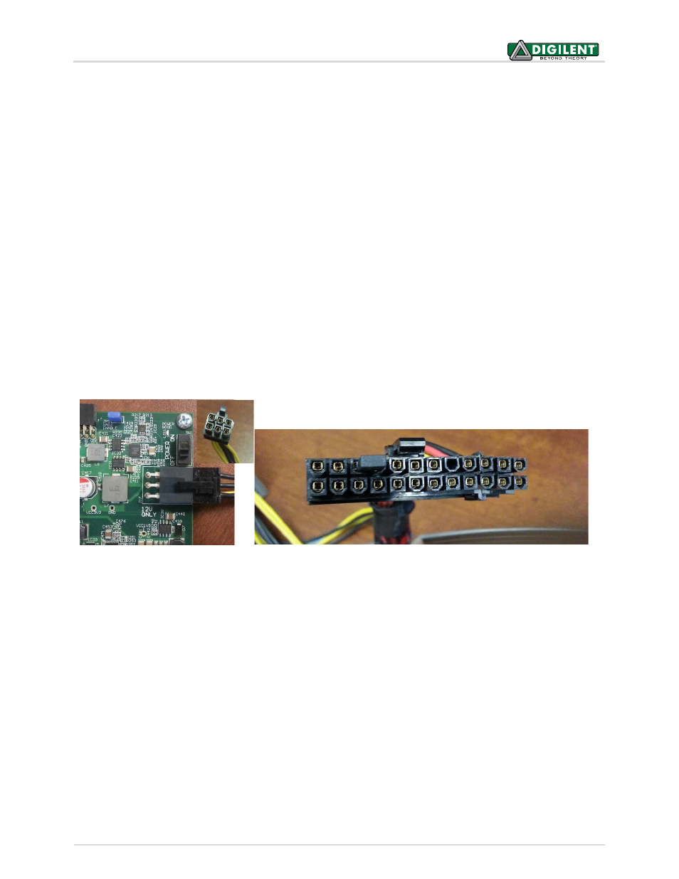
The NetFPGA-1G can be powered using the 6-pin PCIe power supply connector (Fig. 1) of any standard ATX power
supply. When installed on a PC motherboard, you can directly plug the 6-pin PCIe power supply connector of your
PC power supply into J17. When used standalone (without a motherboard), you need to short pins 15 and 16
(pulling down PS_ON signal) of the main 20-pin connector of the standard ATX power supply to power-on the ATX
unit (Fig. 1).
Figure 1. Left: NetFPGA-1G can be powered by plugging the 6-pin PCIe power connector in J17; Right: Pin 16 and 17 are shorted using a jumper
to power on a standard ATX power supply when used standalone.
Analog Devices voltage regulators provide a number of on-board power and reference voltages that are derived
from the main 12V supply, as shown in Table 1. Supply power-on and power-off sequencing follows manufacturer
recommendations. The on-board battery that supports encryption key storage and the real-time clock is charged
when the PCB is powered on and should not need to be replaced during the lifetime of the board.
VADJ controls the signal levels used between the FMC connector and two FPGA Select I/O banks and can be set to
1.2 V, 1.8 V, 2.5 V, or 3.3 V as needed. The board is shipped with the VADJ supply turned off. To turn on VADJ,
jumper JP5 is installed and the FPGA is configured to drive the VADJ_EN pin (AD16) high. The VADJ voltage is
selected via the FPGA configuration using pins AF19 and AF20 as shown in Table 1.
When jumper JP4 is in place, the USB HID connector provides 5V at up to 0.5 A to external USB devices, including
keyboards, mice, and thumb drives. An Analog Devices ADM1177 hot swap controller and power monitor is used
to allow safe device attachment and removal while the board is powered up. The PIC can also measure USB
current and voltage by accessing the on-chip power monitor via the PIC I2C peripheral bus.
Copyright Digilent, Inc. All rights reserved.
Other product and company names mentioned may be trademarks of their respective owners.
Page 5 of 26