1 fpga configuration, Fpga configuration – Digilent 6015-410-001P-KIT User Manual
Page 4

NetFPGA-1G-CML™ Board Reference Manual
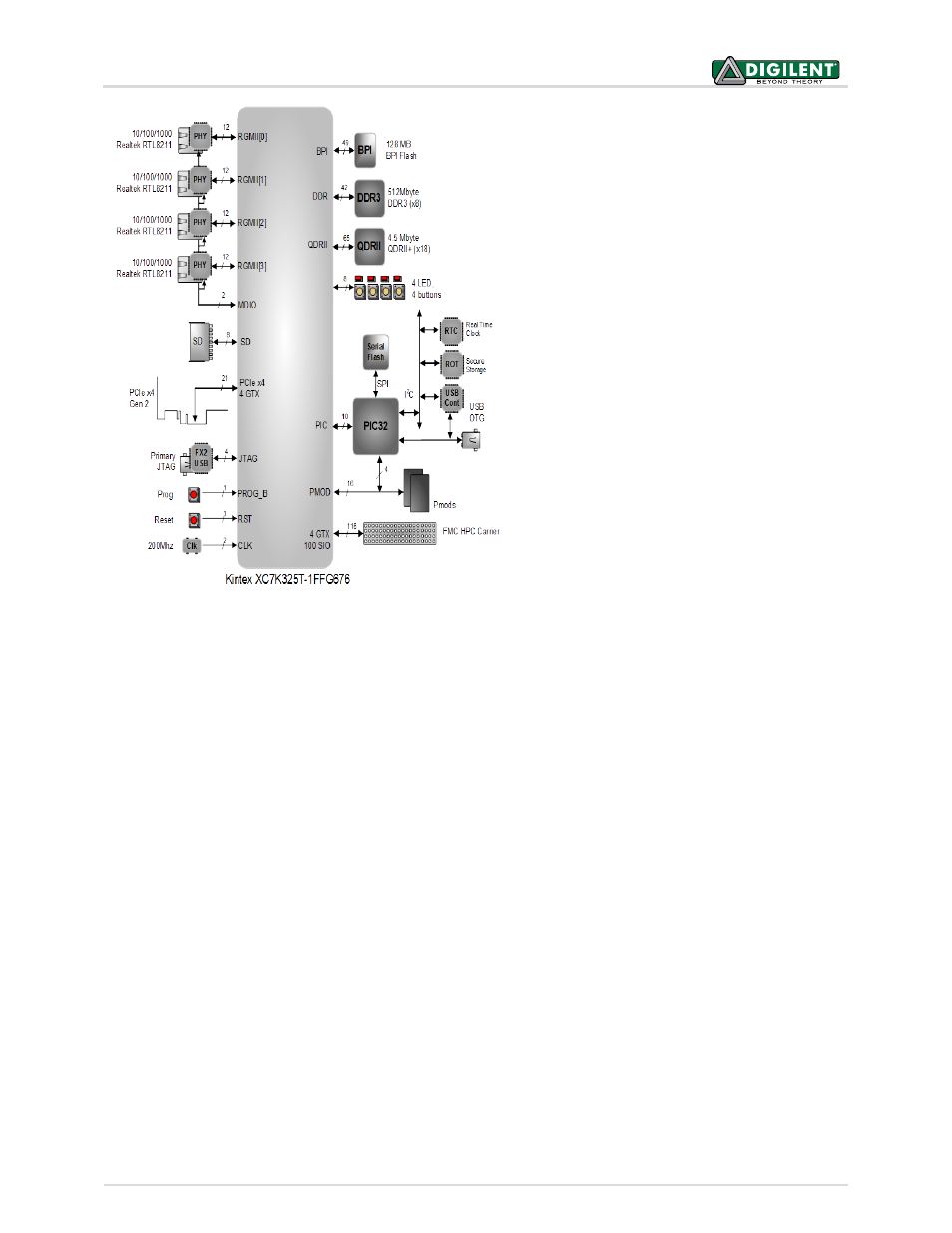
The Kintex-7 XC7K325T-1FFG676 FPGA
has ample logic and I/O capacity for
supporting a wide range of designs with
the following capabilities:
• 50,950 slices, each containing
four 6-input LUTs and eight flip-
flops
• Over 16 Mbit of fast on-chip
block RAM
• Ten clock management tiles with
one PLL and one mixed-mode
clock manager each
• 840 DSP slices
• Integrated PCI Express
• Integrated AES bitstream
encryption and SHA-256
authentication with battery-
backed encryption key
• 400 Select I/O ports (250 high
range, 150 high speed)
• Eight 6.6 Gb/s GTX serial
transceivers
1
FPGA Configuration
The system logic configuration is stored within the FPGA in SRAM-based memory cells. This data defines the
FPGA’s logic functions and circuit connections, but it is volatile since it remains valid only as long as power is
applied. Because of this, the device is configured (i.e., programmed) every time it is turned-on. In addition, it may
also be re-configured at any time power is applied. Once power is removed, the most recently programmed logic
configuration is lost. The configuration data is commonly called a bitstream which is most often contained in files
of type “.bit” or “.mcs”. These files may be created several different ways using Xilinx development software.
The FPGA may be configured from three different sources. These include the on-board BPI flash, an off-board USB
flash drive, or via a PC. The NetFPGA-1G follows a specific configuration sequence when it powers up and comes
out of reset. If a valid “download.bit” file is detected on an attached USB flash drive, that bitstream will be used to
program the FPGA. The flash drive must be FAT formatted, contain a single “download.bit” file, and be attached to
the USB-HOST port (J13) with jumper JP4 in place. If no flash drive bitstream is detected, an attempt will be made
to configure the device from the on-board BPI flash address 0x0. If no flash bitstream is available, the board idles
until it is programmed from a PC. PC programming can be done either via a USB cable connected to the USB PROG
port (J12), or a JTAG programming cable connected to the XILINX PROG CABLE port (J15). Any flash drive
bitstreams that are not built for the Xilinx XC7K325T FPGA will be ignored. This power-on programming sequence
can be re-initiated at any time after power is applied by depressing the red PROG button (BTN5).
Both Digilent and Xilinx distribute free software that can be used to transfer bitstreams from a PC as well as create
bitstream files to load via a flash drive. Digilent’s Adept and Xilinx’s iMPACT applications can directly program the
FPGA using a .bit file via a standard USB A to Micro B cable connected to J12 or through any of several Digilent
JTAG programming cables connected to J15. The on-board BPI flash is programmed via similar means. When
programming the BPI, iMPACT transfers a .mcs format bitstream to the flash in a two-step process. iMPACT first
Copyright Digilent, Inc. All rights reserved.
Other product and company names mentioned may be trademarks of their respective owners.
Page 4 of 26
