Input/output circuit, Input circuit, Output circuit – KEYENCE XG-8000 Series User Manual
Page 8
8
• Use a shield cable that supports an RS-422 signal for the connection to the
IN2 Connector for encoder input, and always connect the Cable shield to
the FG.
• Power source 0 V and COMIN1, COMIN2 (Connector), COMIN2 (Terminal
block), COMOUT1, COMOUT2, COMOUT_F+, COMOUT_F-,
COMOUT2_F+, COMOUT2_F-, and 0VOUT are all isolated.
• COMOUT2_F+ and COMOUT2_F- are the common terminal for dedicated
output for OUT2 Connector 1 through to 4.
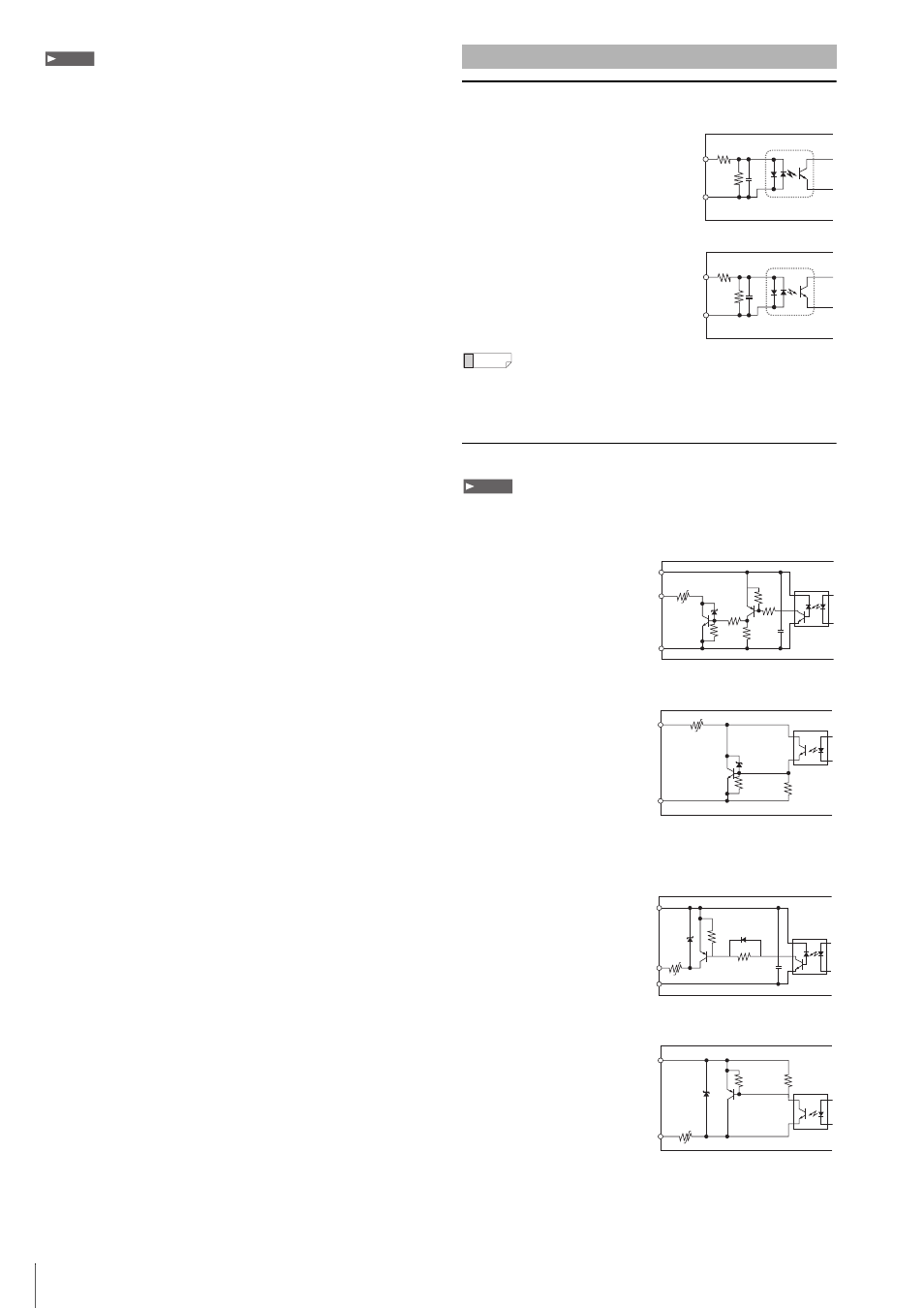
Input Circuit
Input circuit diagram
Circuit A
(compatible with F_IN0 to 7, EV)
• Max. superimposed voltage: 26.4 V
• ON voltage: 10.8 V or greater
• ON current: 3 mA or greater
• OFF voltage: 5 V or less
• OFF current: 1 mA or less
Circuit B (other inputs)
• Max. superimposed voltage: 26.4 V
• ON voltage: 10.8 V or greater
• ON current: 2 mA or greater
• OFF voltage: 3 V or less
• OFF current: 0.3 mA or less
For more details on the common to be connected, see the “Parallel I/O
Interface” (page 6), and “Terminal Block 2 (XG-8500L(P)/8502L(P)/8700L(P)/
8702L(P)/8800(P)/8802(P)/8800L(P)/8802L(P) only)” (page 7).
Output Circuit
The working current of the Poly Switch for the over current is 1 A. Use the
current of 1 A or more for the output.
Output circuit diagram (NPN output type)
Circuit C (F_OUT0 to 7)
• Max. superimposed
voltage: 30 V
• Max. sink current:
50 mA
• Leakage current:
0.1 mA or less
• Residual voltage:
1.4 V or less (50 mA), 1.0 V or less (20 mA)
Circuit D (Other outputs)
• Max. superimposed
voltage: 30 V
• Max. sink current:
50 mA
• Leakage current:
0.1 mA or less
• Residual voltage:
1.4 V or less (50 mA), 1.0 V or less (20 mA)
Output circuit diagram (PNP output type, when the model has P
at the end of the name)
Circuit C (F_OUT0 to 7)
• Max. superimposed
voltage: 30 V
• Max. sink current:
50 mA
• Leakage current:
0.1 mA or less
• Residual voltage:
1.4 V or less (50 mA), 1.0 V or less (20 mA)
Circuit D (Other outputs)
• Max. superimposed
voltage: 30 V
• Max. sink current:
50 mA
• Leakage current:
0.1 mA or less
• Residual voltage:
1.4 V or less (50 mA), 1.0 V or less (20 mA)
Note
Input/Output Circuit
INPUT
COMIN1
or
COMIN2
3.3 k
Ω
10 k
Ω
INPUT
COMIN1
or
COMIN2
6.2 k
Ω
4.7 k
Ω
Reference
Note
10 k
Ω
22 k
Ω
22 k
Ω
22 k
Ω
22 k
Ω
40 V
104
COMOUT_F+
COMOUT_F–
OUTPUT
0.3 A
Poly Switch
10 k
Ω
1 k
Ω
40 V
0.3 A
COMOUT
OUTPUT
Poly Switch
10 k
Ω
22k
Ω
33 V
104
COMOUT_F+
COMOUT_F–
OUTPUT
0.3 A
Poly Switch
10 k
Ω
1 k
Ω
33 V
0.3 A
OUTPUT
Poly Switch
COMOUT