Cypress EZ-OTG CY7C67200 User Manual
Ez-otg™ programmable usb on-the-go, Ez-otg features, Typical applications
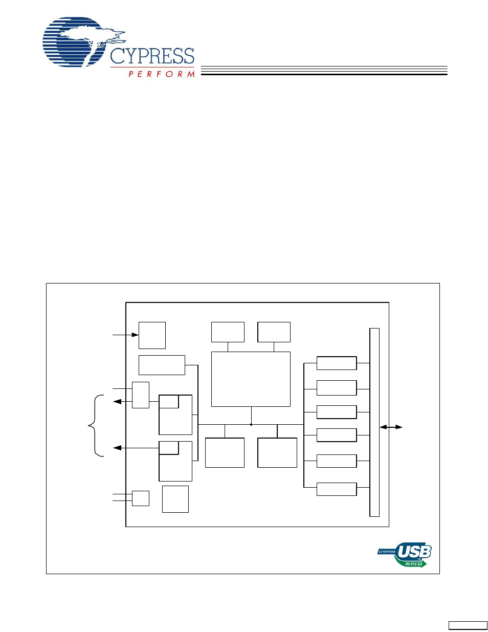
Table of contents
Document Outline
- EZ-OTG Features
- Typical Applications
- Introduction
- Processor Core Functional Overview
- Interface Descriptions
- Power Savings and Reset Description
- Memory Map
- Registers
- Processor Control Registers
- Timer Registers
- General USB Registers
- USB Host Only Registers
- Host n Control Register [R/W]
- Host n Address Register [R/W]
- Host n Count Register [R/W]
- Host n Endpoint Status Register [R]
- Host n PID Register [W]
- Host n Count Result Register [R]
- Host n Device Address Register [W]
- Host n Interrupt Enable Register [R/W]
- Host n Status Register [R/W]
- Host n SOF/EOP Count Register [R/W]
- Host n SOF/EOP Counter Register [R]
- Host n Frame Register [R]
- USB Device Only Registers
- Device n Endpoint n Control Register [R/W]
- Device n Endpoint n Address Register [R/W]
- Device n Endpoint n Count Register [R/W]
- Device n Endpoint n Status Register [R/W]
- Device n Endpoint n Count Result Register [R/W]
- Device n Interrupt Enable Register [R/W]
- Device n Address Register [W]
- Device n Status Register [R/W]
- Device n Frame Number Register [R]
- Device n SOF/EOP Count Register [W]
- OTG Control Registers
- GPIO Registers
- HSS Registers
- HSS Control Register [0xC070] [R/W]
- HSS Baud Rate Register [0xC072] [R/W]
- HSS Transmit Gap Register [0xC074] [R/W]
- HSS Data Register [0xC076] [R/W]
- HSS Receive Address Register [0xC078] [R/W]
- HSS Receive Counter Register [0xC07A] [R/W]
- HSS Transmit Address Register [0xC07C] [R/W]
- HSS Transmit Counter Register [0xC07E] [R/W]
- HPI Registers
- SPI Registers
- SPI Configuration Register [0xC0C8] [R/W]
- SPI Control Register [0xC0CA] [R/W]
- SPI Interrupt Enable Register [0xC0CC] [R/W]
- SPI Status Register [0xC0CE] [R]
- SPI Interrupt Clear Register [0xC0D0] [W]
- SPI CRC Control Register [0xC0D2] [R/W]
- SPI CRC Value Register [0xC0D4] [R/W]
- SPI Data Register [0xC0D6] [R/W]
- SPI Transmit Address Register [0xC0D8] [R/W]
- SPI Transmit Count Register [0xC0DA] [R/W]
- SPI Receive Address Register [0xC0DC [R/W]
- SPI Receive Count Register [0xC0DE] [R/W]
- UART Registers
- Pin Diagram
- Pin Descriptions
- Absolute Maximum Ratings
- Operating Conditions
- Crystal Requirements (XTALIN, XTALOUT)
- DC Characteristics
- AC Timing Characteristics
- Register Summary
- Ordering Information
- Package Diagram