Power savings and reset description, Power savings mode description, Sleep – Cypress EZ-OTG CY7C67200 User Manual
Page 8

CY7C67200
Document #: 38-08014 Rev. *G
Page 8 of 78
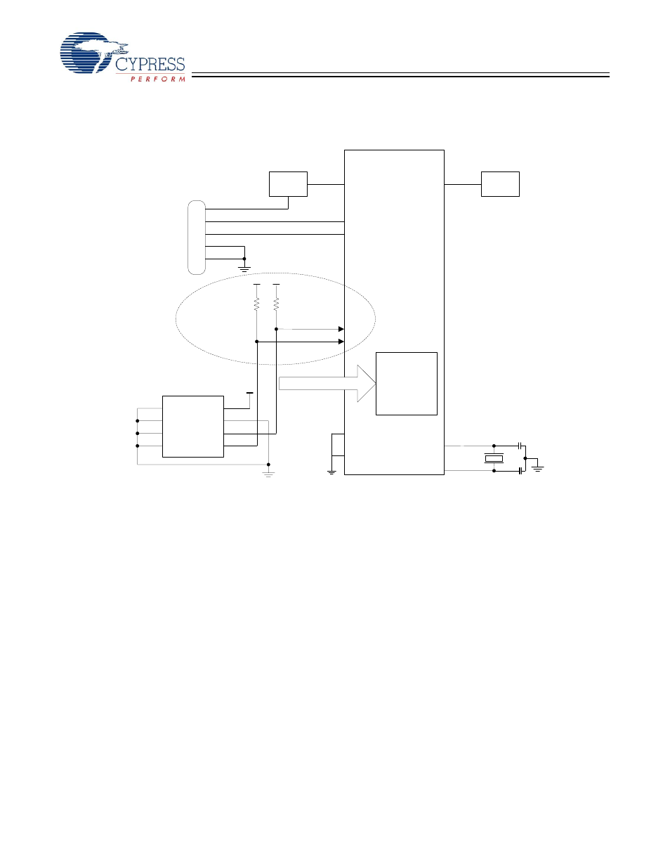
Minimum Hardware Requirements for Standalone Mode – Peripheral Only
Power Savings and Reset Description
The EZ-OTG modes and reset conditions are described in this
section.
Power Savings Mode Description
EZ-OTG has one main power savings mode, Sleep. For
detailed information on Sleep mode;
Sleep mode is used for USB applications to support USB
suspend and non USB applications as the main chip power
down mode.
In addition, EZ-OTG is capable of slowing down the CPU clock
speed through the CPU Speed register [0xC008] without
affecting other peripheral timing. Reducing the CPU clock
speed from 48 MHz to 24 MHz reduces the overall current
draw by around 8 mA while reducing it from 48 MHz to 3 MHz
reduces the overall current draw by approximately 15 mA.
Sleep
Sleep mode is the main chip power down mode and is also
used for USB suspend. Sleep mode is entered by setting the
Sleep Enable (bit 1) of the Power Control register [0xC00A].
During Sleep mode (USB Suspend) the following events and
states are true:
• GPIO pins maintain their configuration during sleep (in
suspend).
• External Memory Address pins are driven low.
• XTALOUT is turned off.
• Internal PLL is turned off.
• Firmware must disable the charge pump (OTG Control
register [0xC098]) causing OTGVBUS to drop below 0.2V.
Otherwise OTGVBUS will only drop to V
CC
– (2 schottky
diode drops).
• Booster circuit is turned off.
• USB transceivers is turned off.
• CPU suspends until a programmable wakeup event.
Figure 5. Minimum Standalone Hardware Configuration – Peripheral Only
EZ-OTG
CY7C67200
GPIO[30]
GPIO[31]
SCL*
SDA*
10k
Bootstrap Options
Bootloading Firmware
*Bootloading begins after POR + 3ms BIOS bootup
Vcc
10k
Vcc
A2
GND
A0
A1
SCL
SDA
VCC
WP
VCC
Up to 64k x8
EEPROM
*GPIO[31:30] 31 30
Up to 2k x8 SCL SDA
>2k x8 to 64k x8 SDA SCL
Int. 16k x8
Code / Data
XOUT
XIN
12MHz
22pf
22pf
nRESET
Reset
Logic
* Parallel Resonant
Fundamental Mode
500uW
20-33pf ±5%
VCC, AVCC,
BoostVCC
VReg
DMinus
DPlus
Standard-B
or Mini-B
D+
VBus
GND
D-
SHIELD
Reserved
GND, AGND,
BoostGND
