An372, Figure 4a. fet drain voltage, Figure 4b. current through fet q4 and diode d3 – Cirrus Logic AN372 User Manual
Page 9
AN372
AN372REV1
9
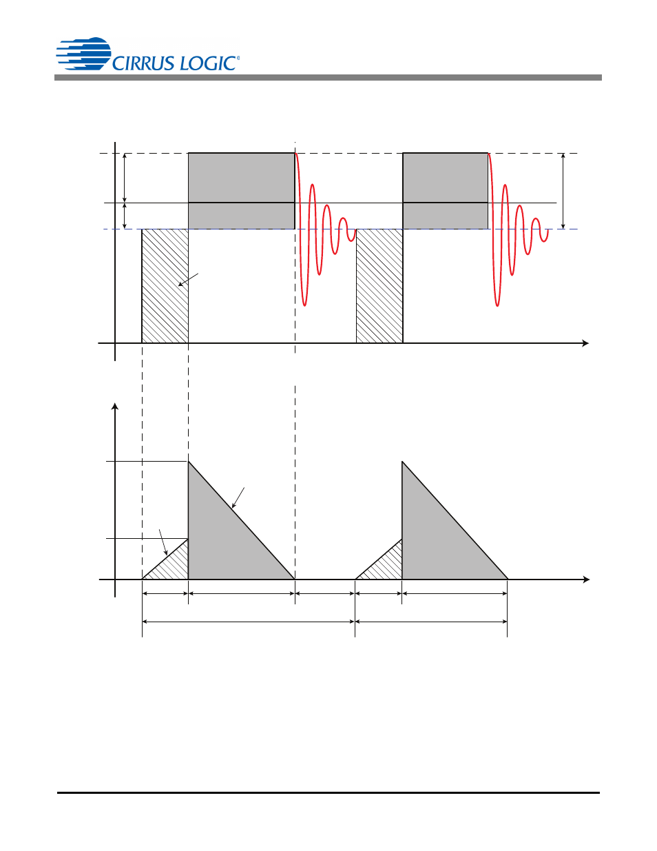
The buck stage is supplied by the boost output voltage. The boost output voltage is regulated within 10% by
the boost stage. The buck control loop regulates the output current as long as the peak current has sufficient
margin to rise 10% at the lowest boost output voltage. Figure 4a and Figure 4b show idealized waveforms of
the FET Q4 drain voltage and drain current and the diode D3 current.
Area = N
ު V
OUT
ު T2
Area = V
OUT
ު T2
Area = (V
BST
- V
OUT
)
ު T1
V
BST
V
ZERO
N
ު V
OUT
V
OUT
t
V
Reflected
Figure 4a. FET Drain Voltage
T1
TT
T3
'
C
1-
'
C
T2
1
I
PK(FB)
t
(N+1)
ު I
PK(FB)
I1
I2
Figure 4b. Current Through FET Q4 and Diode D3
See also other documents in the category Cirrus Logic Hardware:
- CobraNet (147 pages)
- CS4961xx (54 pages)
- CS150x (8 pages)
- CS1601 (2 pages)
- CS1501 (16 pages)
- CS1601 (16 pages)
- CS1610 (16 pages)
- CRD1610-8W (24 pages)
- CRD1611-8W (25 pages)
- CDB1610-8W (21 pages)
- CS1610A (18 pages)
- CDB1611-8W (21 pages)
- CDB1610A-8W (21 pages)
- CDB1611A-8W (21 pages)
- CRD1610A-8W (24 pages)
- CRD1611A-8W (25 pages)
- CS1615 (16 pages)
- AN403 (15 pages)
- AN401 (14 pages)
- AN400 (15 pages)
- AN375 (27 pages)
- AN376 (9 pages)
- CRD1615-8W (22 pages)
- CRD1616-8W (23 pages)
- AN402 (14 pages)
- AN404 (15 pages)
- CRD1615A-8W (21 pages)
- CS1615A (16 pages)
- CS1630 (56 pages)
- AN374 (35 pages)
- AN368 (80 pages)
- CRD1630-10W (24 pages)
- CRD1631-10W (25 pages)
- CS1680 (16 pages)
- AN405 (13 pages)
- AN379 (31 pages)
- CRD1680-7W (31 pages)
- AN335 (10 pages)
- AN334 (6 pages)
- AN312 (14 pages)
- AN Integrating CobraNet into Audio Products (16 pages)
- CobraNet Audio Routing Primer (9 pages)
- Bundle Assignments in CobraNet Systems (3 pages)
- CS2300-01 (3 pages)
- CS2000-CP (38 pages)