3 buck stage design, An372 – Cirrus Logic AN372 User Manual
Page 6
AN372
6
AN372REV1
3.3 Buck Stage Design
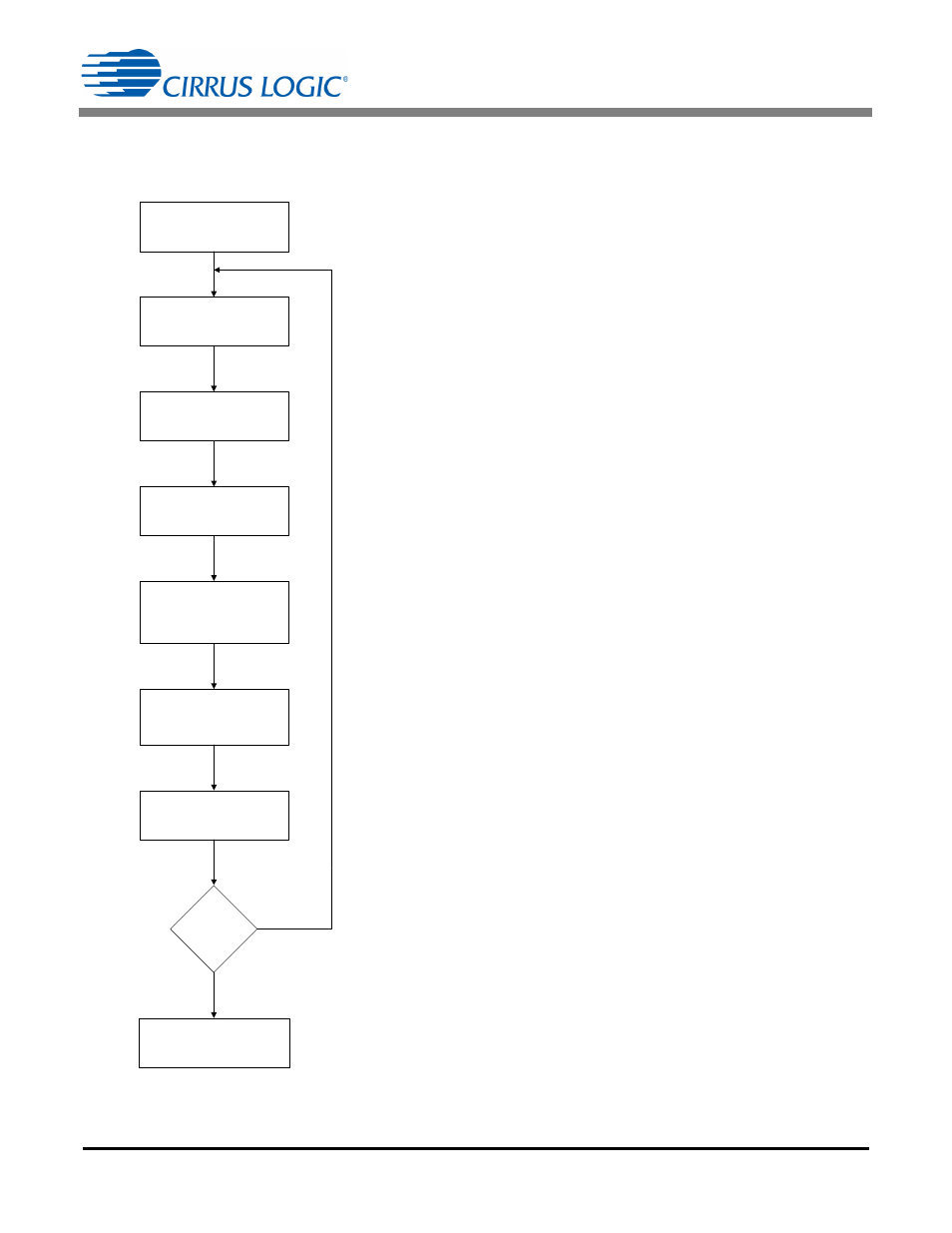
Figure 2 illustrates the steps for designing the buck stage.
Figure 2. Buck Stage Design
Buck Specification
Determine N, F
sw
,
V
Reflected
, and V
CLAMP
Estimate T3
Calculate TT
fb
Calculate R
Sense
,
R
FBGAIN
, and Buck
Inductance
R
Sense
,R
FBGAIN
Fit?
Yes
No
Calculate T1,
T2, and I
PK(FB )
Calculate RMS Current
and Output Capacitor
Buck Inductor
Specification
Steps for the Buck Design
1. Select a buck topology
2. Set the boost output voltage, V
BST
.
3. Select a FET that aligns with the quality standards of the
designer’s company.
4. Determine the inductor turns ratio from the
V
BST
, FET
voltage, and reflected voltage, V
Reflected
.
5. Use the nominal switching frequency and an initial
estimate for time T3 to determine the value of time TT at
full brightness.
6. Use V
BST
, TT, and V
Reflected
to determine times T1 and T2.
7. Use times T2 and TT, turns ratio N, and load current to
determine the value of the peak primary current, I
PK(FB)
.
8. Use I
PK(FB)
to determine R
Sense
.
9. Calculate the buck inductance L using time T1.
10. Calculate second stage gain resistor R
FBGAIN
using full
load conditions. Ensure linearity of the load versus the dim
curve.
11. Calculate RMS currents in the two windings of L using
peak current I
PK(FB)
and duty cycle.
12. Select an output capacitor.
13. Determine the buck inductor specifications.
14. Determine if the buck inductor fits into a specified form
factor after designing and constructing the buck inductor.
Repeat steps 3 to 12 until form factor criteria is met.
15. Refinements to the circuit with final buck inductor design.
16. Validate that the system meets the operating criteria.