An372 – Cirrus Logic AN372 User Manual
Page 15
AN372
AN372REV1
15
Step 14) Circuit Adjustments
Circuit adjustments are required after the inductor has been designed and constructed. Recalculate resistor
R
FBGAIN
using Equation 16.
The second-stage gain, FB
Gain
, is an internal constant that is programmable by resistor R
FBGAIN.
FB
Gain
is used in the second-stage algorithm to control the switching period, TT. The range of FB
Gain
is limited to
:
which has the following implications:
If FB
Gain
is close to 1, the duty cycle will be low, which will cause a low reflected voltage, V
Reflected
. In this
situation, a high I
PK(FB)
current is required to reach full brightness, and the only advantage would be to lower
the FET breakdown voltage. If the value of FB
Gain
were in the range of 2 to 2.5, then V
Reflected
would be in the
range of V
BST
to (1.5
V
BST
), resulting in a duty cycle that is between 50% and 60%. This setting causes a
lower I
PK(FB)
, requiring a higher FET breakdown voltage.
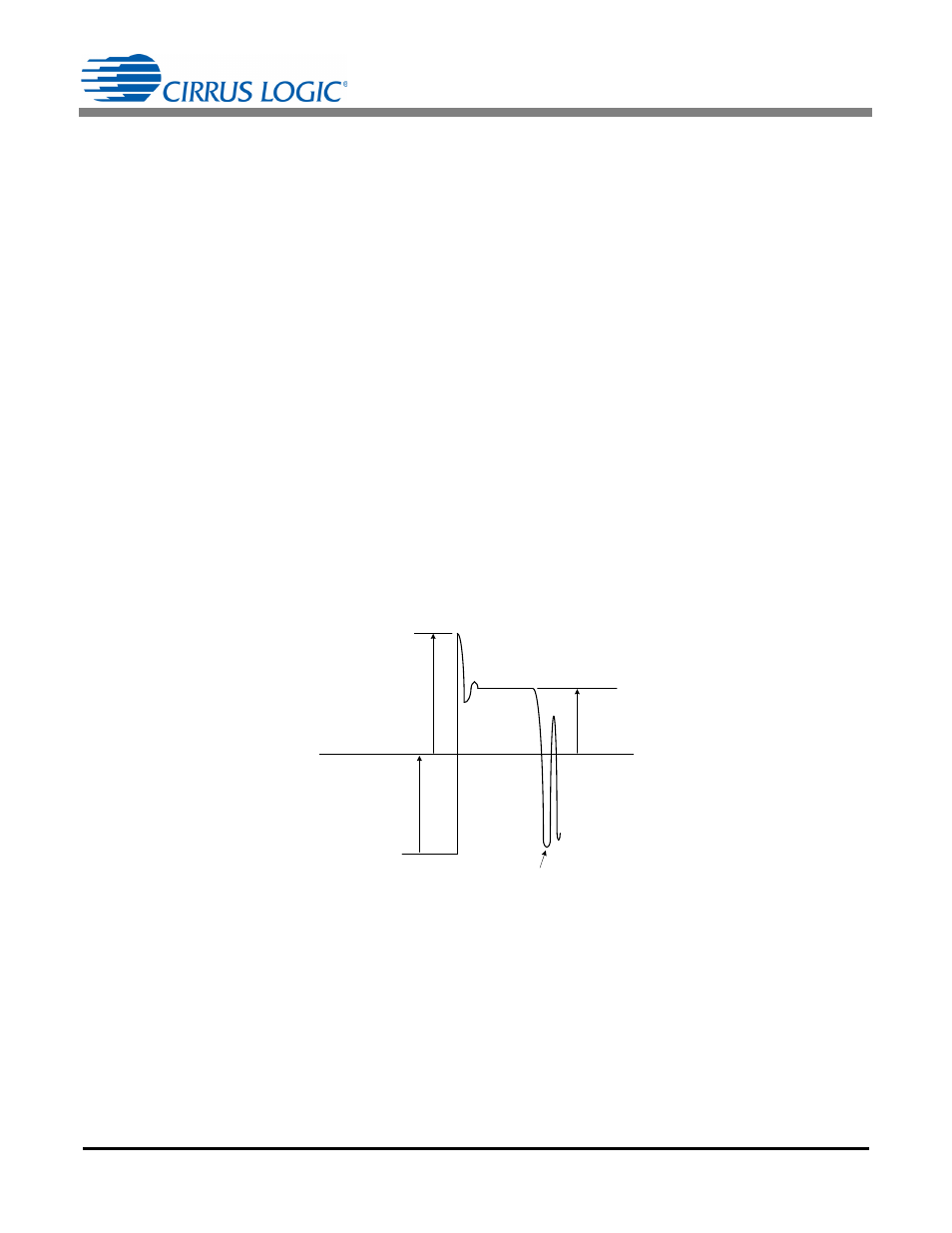
The duration of time T1 is determined by the time it takes the primary current to reach I
PK(FB)
, and the duration
of time T2 is dependent on the time it takes the secondary current to reach 0. To achieve the best full-power
efficiency, adjust the switching period, TT, which will start a new switching cycle after the buck FET drain
voltage has reached the valley (see Figure 7). Once the buck inductor is built, R
FBGAIN
can be adjusted to
change TT to allow it to cycle at the valley. Adjusting R
FBGAIN
changes the switching frequency slightly.
Although R
FBGAIN
could be used to control the load current, its primary purpose is to control the valley
switching range. It is recommended to adjust the load current by changing the primary current sense resistor,
R
Sense
, connected to the FBSENSE pin of the IC, and then use R
FBGAIN
to control valley switching.
Step 15) Recalculate R
Sense
The buck primary current is controlled by comparing the voltage across R
Sense
at pin FBSENSE to an internal
threshold of 1.4V. To guarantee the rated LED current under worst-case conditions, when the LED string has
maximum voltage, the V
BST
is at its minimum point, and R
Sense
is at its highest tolerance. Adjust R
Sense
to
obtain the nominal LED current, then adjust R
FBGAIN
to hit the valley.
FB
Gain
TT
fb
T2
fb
------------
V
BST
N V
OUT
+
V
BST
V
OUT
–
--------------------------------------------------
=
=
[Eq. 20]
1 FB
Gain
2.5
[Eq. 21]
T2
fb
TT
fb
2.5 T
2
fb
0 V
Reflected
1.5 V
BST
15.6k
R
FBGAIN
62.5k
[Eq. 22]
First Valley
Buck FET
Voltage
V
CLAMP
V
BST
V
Reflected
Figure 7. Switching Waveform of Buck FET Drain