An372 – Cirrus Logic AN372 User Manual
Page 8
AN372
8
AN372REV1
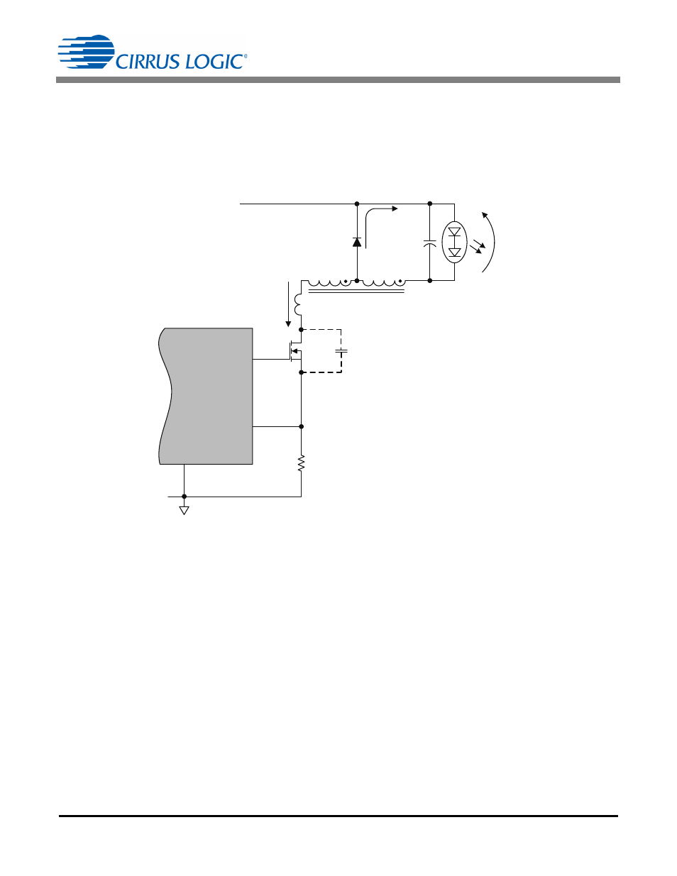
Figure 3 illustrates a generic implementation of a buck converter using a tapped inductor topology. A normal
buck stage can be implemented by neglecting the N turn's extension. The load is composed of a string of
LEDs. Diode D3 is the catch diode, also known as the free wheeling diode, and its function is to allow the
current to flow in inductor L4 and to the load after FET Q4 opens. Capacitance C
P
represents the combined
parasitic capacitance associated with the FET drain node, usually consisting of the FET drain-source
capacitance, inductor winding capacitance, diode D3 reverse bias capacitance, and any additional snubbing
capacitance that may be required.
Leakage inductance, represented by L
K
, is inevitably associated with a tapped inductor. Inductor windings
labeled N turns and 1 turn are tightly coupled; the stray flux is represented by the uncoupled inductance L
K
.
Leakage inductance L
K
is not a concern in a normal buck (non-tapped) design. Inductor winding N and 1 are
the normalized winding turns. The real inductor will have T turns and (N
T) turns.
C5
R21
Q4
GND
GD
FBSENSE
CS1612/13
V
BST
D3
L4
I1
V
OUT
N:1
C
P
I2
L
K
N turns
1 turn
Figure 3. Buck Converter