Figure 6), An372 – Cirrus Logic AN372 User Manual
Page 12
AN372
12
AN372REV1
current flows in the load circuit, dilutes the energy delivered during time T1 and T2 resulting in lower average
power to the load.
Dimming Operation
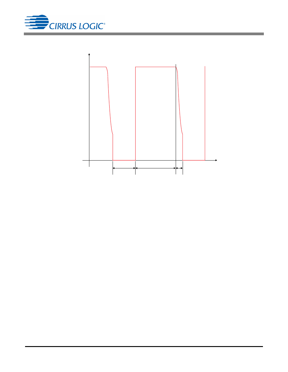
The dimmer conduction time or phase cut information is extracted by the boost stage and supplied to the buck
stage as a digital parameter, dim, ranging from 0.02 to 1 as a measure of the normalized output power to be
delivered. The dim parameter controls both the normalized peak current in the inductor and the total period
TT. Reaching a lower peak current requires less time T1 and consequently less time T2 to discharge the
inductor; at the same time, the idle time T3 is increased to keep the total period TT nearly constant. Doing so
reduces power, maintaining constant frequency, until the peak current is halved. Further power reduction is
obtained increasing the period TT without reducing the current.
When the current is moderately reduced, time T3 is increased just enough before turning ‘ON’ FET Q4 during
the second or third valley sustaining the quasi-resonant mode of operation. At deeper dimming levels, reducing
the switching frequency also reduces the capacity losses; therefore, enforcing a quasi-resonant mode is no
longer a requirement, and the oscillatory transient is left to decay until a new cycle is started at the calculated
TT.
Basic Design Equation
The DC voltage across any winding must be zero. The entire winding (N+1) is subject to voltage (V
BST
- V
OUT
)
during time T1 and subject to voltage ((N+1) x V
OUT
) during time T2. The average voltage across L is
calculated using Equation 6:
Solving Equation 6 for ratio T2/T1:
T1
T2
T3
V
DS
t
Figure 6. Timing Diagram of Times T1, T2, T3, and TT
V
BST
V
OUT
–
T1
N 1
+
V
OUT
T2
–
0
=
[Eq. 6]
T2
T1
-------
V
BST
V
OUT
–
N 1
+
V
OUT
----------------------------------------
=
[Eq. 7]