An372 – Cirrus Logic AN372 User Manual
Page 7
AN372
AN372REV1
7
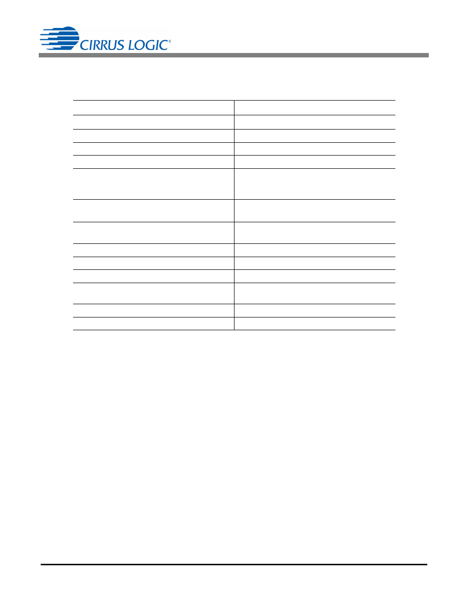
Step 1) Choosing a Buck Topology
The first step in designing the buck stage is to choose a tapped buck or a normal buck. Consider the following
advantages and disadvantages of either solution:
The tapped buck is best suited for a high V
BST
/V
OUT
ratio. The best approach to guarantee the most
convenient buck topology choice is to complete a preliminary design for both, and then determine whether
parameter results are impractical or out of range for the available technology and cost constraints.
Normal Buck
Tapped Buck
Most effective with low V
BST
/V
OUT
ratios
Most effective with high V
BST
/V
OUT
ratios
High peak current; low duty cycle
Low peak current; high duty cycle
Simple low-value inductor
Two windings of different turns and gauges
Reduced quasi-resonant advantage
Take advantage of the near zero-voltage switching
Leakage inductance L
K
losses are not an issue, so
no snubber is required
Leakage inductance L
K
losses may require a
snubber but may self-snub by the inductor winding
capacitance
Low inductance L allows for high oscillation
frequency
High inductance L and high parasitic capacitance
C
P
gives low oscillation frequency
Load current has lower RMS ripple and no
discontinuity; visualize Figure 1 for N=0.
Load current has higher RMS ripple and a
discontinuity step; see Figure 1
Higher bulk capacitor ripple current
Lower bulk capacitor ripple current
Higher bulk capacitor value
Lower bulk capacitor value
Higher conduction losses
Lower conduction losses
May be bound by minimum switching period T1
limitations
Switching period T1 can be extended proportionally
to turns ratio N
Lower FET voltage stress
Higher FET voltage stress
Higher FET current stress
Lower FET current stress