3 reset operation, 4 led indicators, Media independent interface (mii) – Cirrus Logic CS8952 User Manual
Page 25: 3 reset operation 3.4 led indicators, Cs8952
CS8952
CrystalLAN™ 100BASE-X and 10BASE-T Transceiver
25
DS206F1
Auto-Negotiation encapsulates information within
a burst of closely spaced Link Integrity Test Pulses,
referred to as a Fast Link Pulse (FLP) Burst. The
FLP Burst consists of a series of Link Integrity
Pulses which form an alternating clock / data se-
quence. Extraction of the data bits from the FLP
Burst yields a Link Code Word which identifies the
capability of the remote device.
In order to support legacy 10 and 100 Mb/s devic-
es, the CS8952 also supports parallel detection. In
parallel detection, the CS8952 monitors activity on
the media to determine the capability of the link
partner even without auto-negotiation having oc-
curred.
3.3
Reset Operation
Reset occurs in response to six different conditions:
1) There is a chip-wide reset whenever the RE-
SET pin is high for at least 200 ns. During a
chip-wide reset, all circuitry and registers in the
CS8952 are reset.
2) When power is applied, the CS8952 maintains
reset until the voltage at the VDD supply pins
reaches approximately 3.6 V. The CS8952
comes out of reset once VDD is greater than ap-
proximately 3.6 V and the crystal oscillator has
stabilized.
3) There is a chip-wide reset whenever the RE-
SET bit (bit 15 of the Basic Mode Control Reg-
ister (address 00h)) is set.
4) Digital circuitry is reset whenever bit 0 of the
PCS Sub-Layer Configuration Register (ad-
dress 17h) is set. Analog circuitry is unaffected.
5) Analog circuitry is reset and recalibrated when-
ever the CS8952 enters or exits the power-
down state, as requested by pin PWRDN.
6) Analog circuitry is reset and recalibrated when-
ever the CS8952 changes between 10 Mb/s and
100 Mb/s modes.
After a reset, the CS8952 latches the signals on var-
ious input pins in order to initialize key registers
and goes through a self configuration. This in-
cludes calibrating on-chip analog circuitry. Time
required for the reset calibration is typically 40 ms.
External circuitry may access registers internal to
the CS8952 during this time. Reset and calibration
complete is indicated when bit 15 of the Basic
Mode Control Register (address 00h) is clear.
3.4
LED Indicators
The LEDx, SPD100, and SPD10 output pins pro-
vide status information that can be used to drive
LEDs or can be used as inputs to external control
circuitry. Indication options include: receive activ-
ity, transmit activity, collision, carrier sense, polar-
ity OK, descrambler synchronization status, auto-
negotiation status, speed (10 vs. 100), and duplex
mode.
4. MEDIA INDEPENDENT INTERFACE
(MII)
The Media Independent Interface (MII) provides a
simple interconnect to an external Media Access
Controller (MAC). This connection may be chip to
chip, motherboard to daughterboard, or a connec-
tion between two assemblies attached by a limited
length of shielded cable and an appropriate connec-
tor.
The MII interface uses the following pins:
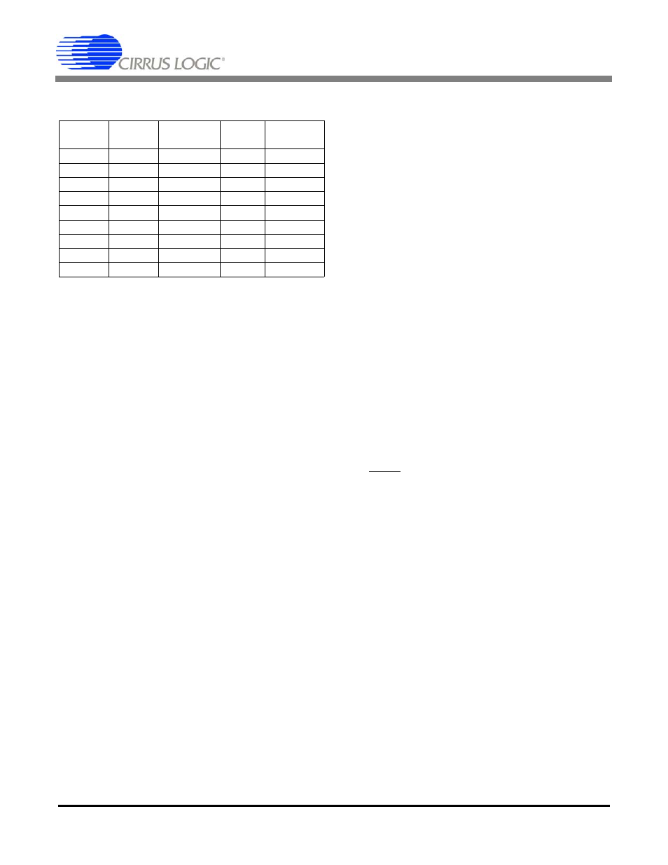
AN1
AN0
Forced/
Auto
Speed
(Mb/s)
Full/Half
Duplex
Low
Floating
Forced
10
Half
High
Floating
Forced
10
Full
Floating
Low
Forced
100
Half
Floating
High
Forced
100
Full
Floating
Floating
Auto-Neg
100/10
Full/Half
Low
Low
Auto-Neg
10
Half
Low
High
Auto-Neg
10
Full
High
Low
Auto-Neg
100
Half
High
High
Auto-Neg
100
Full
Table 5.