8 voltage reference, 9 system initialization, 10 power-down states – Cirrus Logic CS5461A User Manual
Page 20: 11 oscillator characteristics, Figure 8. oscillator connection, Cs5461a
CS5461A
20
DS661F3
The Cycle Count Register (N) must be set to a value
greater than one. Status bit TUP in the Status Register,
indicates when the Temperature Register is updated.
The Temperature Offset Register sets the zero-degree
measurement. To improve temperature measurement
accuracy, the zero-degree offset should be adjusted af-
ter the CS5461A is initialized. Temperature offset cali-
bration is achieved by adjusting the Temperature Offset
Register (T
off
) by the differential temperature (
T) mea-
sured from a calibrated digital thermometer and the
CS5461A temperature sensor. A one-degree adjust-
ment to the Temperature Register (T) is achieved by
adding 2.737649x10
-4
to the Temperature Offset Regis-
ter (T
off
). Therefore,
if T
off
= -0.0951126 and
T = -2.0 (
o
C), then
or 0xF3C168 (2’s compliment notation) is stored in the
Temperature Offset Register (T
off
).
To convert the Temperature Register (T) from a Celsius
scale (
o
C) to a Fahrenheit scale (
o
F) utilize the formula
Applying the above relationship to the CS5461A tem-
perature measurement algorithm
If T
off
= -0.09566 and T
gain
= 23.507 for a Celsius
scale, then the modified values are T
off
= -0.0907935
(0xF460E1) and T
gain
= 42.3132 (0x54A05E) for a
Fahrenheit scale.
5.8 Voltage Reference
The CS5461A is specified for operation with a +2.5 V
reference between the VREFIN and AGND pins. To uti-
lize the on-chip 2.5 V reference, connect the VREFOUT
pin to the VREFIN pin of the device. The VREFIN pin
can be used to connect external filtering and/or refer-
ences.
5.9 System Initialization
Upon powering up, the digital circuitry is held in reset
until the analog voltage reaches 4.0 V. At that time, an
eight-XIN-clock-period delay is enabled to allow the os-
cillator to stabilize. The CS5461A will then initialize.
A hardware reset is initiated when the RESET pin is as-
serted with a minimum pulse width of 50 ns. The
RESET signal is asynchronous, with a Schmitt-trigger
input. Once the RESET pin is de-asserted, an
eight-XIN-clock-period delay is enabled.
A software reset is initiated by writing the command of
0x80. After a hardware or software reset, the internal
registers (some of which drive output pins) will be reset
to their default values. Status bit DRDY in the Status
Register, indicates the CS5461A is in its active state
and ready to receive commands.
5.10 Power-down States
The CS5461A has two power-down states, stand-by
and sleep. In the stand-by state all circuitry except the
voltage reference and crystal oscillator is turned off. To
return the device to the active state a power-up com-
mand is sent to the device.
In sleep state all circuitry except the instruction decoder
is turned off. When the power-up command is sent to
the device, a system initialization is performed (see
Section 5.9 System Initialization
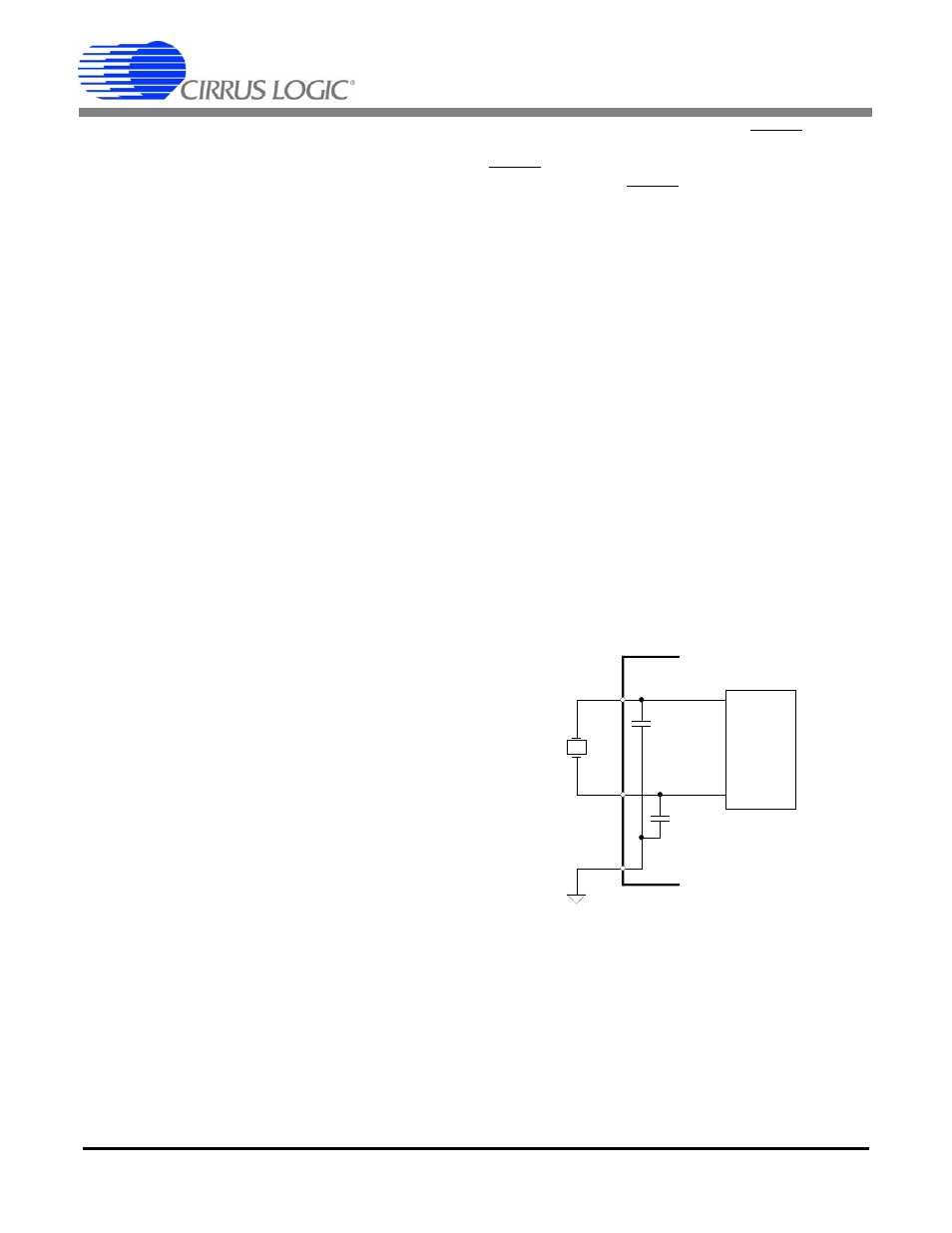
5.11 Oscillator Characteristics
The XIN and XOUT pins are the input and output of an
inverting amplifier configured as an on-chip oscillator,
as shown in Figure 8. The oscillator circuit is designed
to work with a quartz crystal. To reduce circuit cost, two
load capacitors C1 and C2 are integrated in the device,
from XIN to DGND, and XOUT to DGND. PCB trace
lengths should be minimized to reduce stray capaci-
tance. To drive the device from an external clock
source, XOUT should be left unconnected while XIN is
driven by the external circuitry. There is an amplifier be-
tween XIN and the digital section which provides
CMOS-level signals. This amplifier works with sinusoi-
T
off
T
off
T
+
2.737649
10
4
–
=
T
off
0.0951126
2.0
–
+
2.737649
10
4
–
–
0.09566
–
=
=
F
o
9
5
---
C
o
17.7778
+
=
T
F
o
9
5
---
T
gain
T
C
o
T
off
17.7778
2.737649
10
4
–
+
+
=
Oscillator
Circuit
DGND
XIN
XOUT
C1
C1 =
22 pF
C2
C2 =
Figure 8. Oscillator Connection