3 clock and data flow for usb data delivery, Figure 1-5. hdmi clocking -8, Table 1-2. s/pdif clocking -8 – Cirrus Logic CRD49530-USB User Manual
Page 13
CRD49530-USB System Description
CRD49530-USB User’s Manual
DS705RD3
Copyright 2008 Cirrus Logic
1-8
The CS4953xx always masters its output clocks (DSP_SCLK/DSP_LRCLK).
Note: MUXED_MCLK is the clock signal that is driven by the CS8416’s RMCK pin. The CS8416
provides the recovered clock from the S/PDIF input unless it loses signal lock, in which case the
CS8416 passes the DSP clock (XTAL_OUT) that it receives on the OMCK pin.
1.3.10.3 Clock and Data Flow for USB Data Delivery
This feature is used by engineering development and debugging purposes.
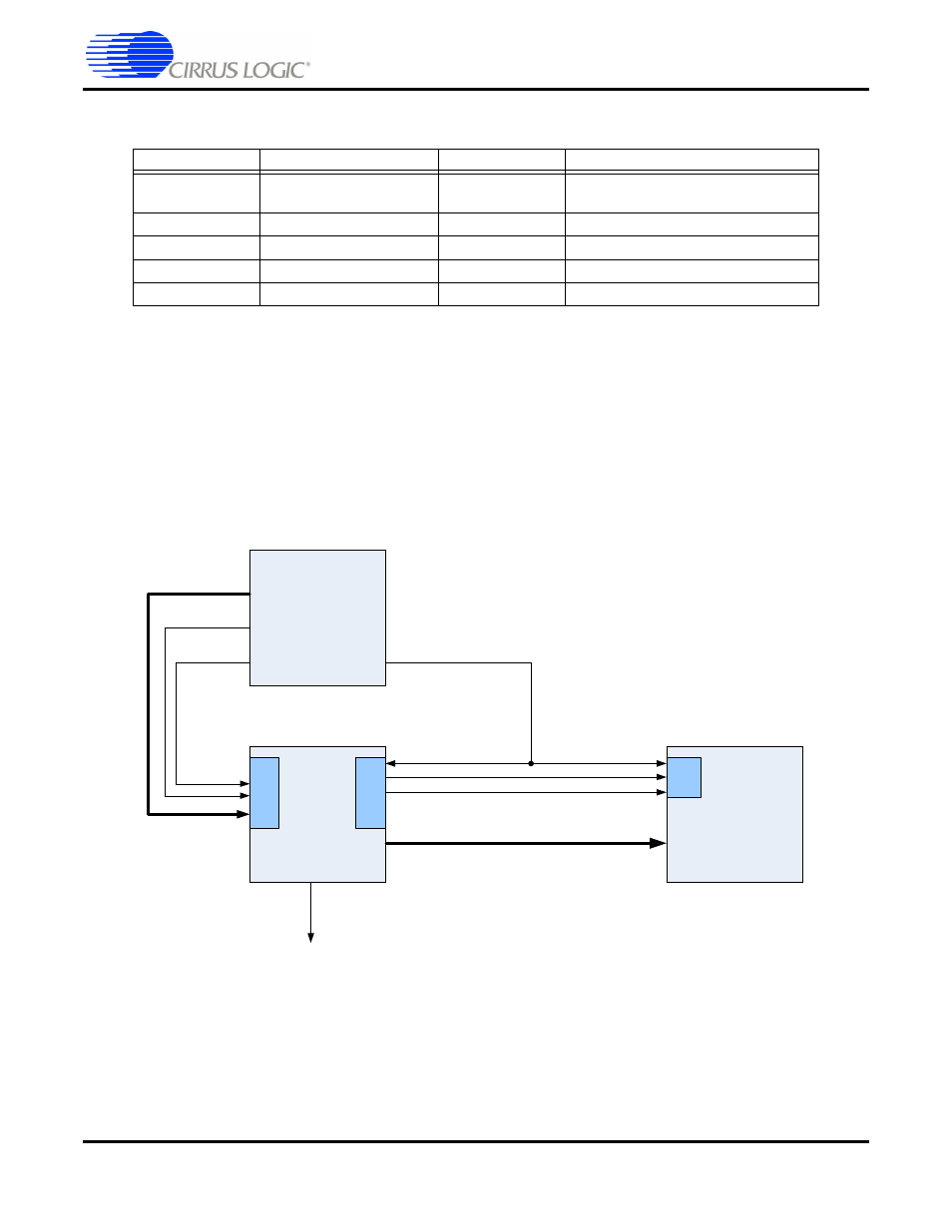
Figure 1-5. HDMI Clocking
When the audio input source multiplexer (U1, U2) is used to select HDMI clocks and data, the HDMI
source masters the system MCLK, and the input clocks (MUXED_SCLK/MUXED_LRCLK) of the
CS4953xx.
Table 1-2. S/PDIF Clocking
Clock Name
Clock Master Source
Clock Driver
Clock Frequency
MUXED_MCLK
CS8416
CS8416
256*S/PDIF Fs
(e.g. 12.288 MHz for 48 kHz)
MUXED_SCLK
MUXED_MCLK
CS8416
64*Input Fs (default)
MUXED_LRCLK
MUXED_MCLK
CS8416
Input Fs
DSP_SCLK
MUXED_MCLK
CS4953xx
64*Output Fs (default)
DSP_LRCLK
MUXED_MCLK
CS4953xx
1*Input Fs (default)
CS4953xx
CS42448
HDMI
SOURCE
MUXED_SCLK
DSP_SCLK
DSP_LRCLK
MUXED_LRCLK
MUXED_DAI[4:0]
DSP_DA0[3:0]
X
M
T
A S/
PDIF
O
UT
MUXED_MCLK
DAI
DAO
SDIN