2 clock and data flow for s/pdif input, Figure 1-4. s/pdif clocking -7, Table 1-1. adc clocking -7 – Cirrus Logic CRD49530-USB User Manual
Page 12
1-7
Copyright 2008 Cirrus Logic
DS705RD3
CRD49530-USB System Description
CRD49530-USB User’s Manual
The CS4953xx always masters its output clocks (DSP_SCLK/DSP_LRCLK).
Note: MUXED_MCLK is the clock signal that is driven by the CS8416’s RMCK pin. The CS8416
provides the recovered clock from the S/PDIF input unless it loses signal lock, in which case the
CS8416 passes the DSP clock (XTAL_OUT) that it receives on the OMCK pin.
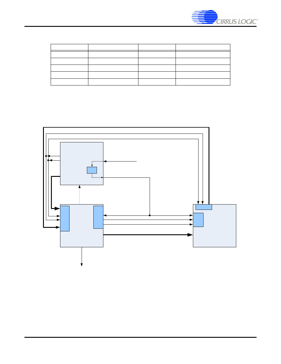
1.3.10.2 Clock and Data Flow for S/PDIF Input
Figure 1-4. S/PDIF Clocking
The S/PDIF clocking architecture is used when any S/PDIF RX is used as an audio source, whether S/
PDIF is the only audio input or is used at the same time as ADC audio (i.e. any S/PDIF RX is selected as
described in "
USB (I2S) Audio Input" on page 4-5
), and the audio input source multiplexer (U1, U2) is
used to select on-board audio sources.
illustrates this clocking configuration.
MCLK recovered from the incoming S/PDIF stream must be MCLK for the system, and the codec masters
the input clocks (MUXED_SCLK/MUXED_LRCLK) of the CS4953xx. In this configuration the internal
multiplexer of the CS8416 routes the recovered MCLK to MUXED_MCLK.
Table 1-1. ADC Clocking
Clock Name
Clock Master Source
Clock Driver
Clock Frequency
MUXED_MCLK
CS4953xx
CS8416
24.576 MHz
MUXED_SCLK
MUXED_MCLK
CS42448
64*Input Fs (default)
MUXED_LRCLK
MUXED_MCLK
CS42448
Input Fs
DSP_SCLK
MUXED_MCLK
CS4953xx
64*Output Fs (default)
DSP_LRCLK
MUXED_MCLK
CS4953xx
1*Input Fs (default)
CS4953xx
CS42448
CS8416
MUXED_SCLK
DSP_SCLK
DSP_LRCLK
DS
P_D
A
I4
MUXED_LRCLK
MUXED_DAI[3:0]
XTA
L
_OU
T
S/PDIF Input
DSP_DA0[3:0]
X
MT
A S/
P
D
IF
O
UT
MUXED_MCLK
DAI
DAO
SDIN
SDOUT
PLL