10 audio clocking, 1 clock and data flow for adc input, 10 audio clocking -6 – Cirrus Logic CRD49530-USB User Manual
Page 11: Figure 1-3. adc clocking -6, Audio
CRD49530-USB System Description
CRD49530-USB User’s Manual
DS705RD3
Copyright 2008 Cirrus Logic
1-6
but Cirrus recommends using serial flash for all systems. Adding a parallel flash makes the routing of the
SDRAM bus much more complicated.
1.3.10 Audio Clocking
Clocking architecture is one of the most important aspects of an audio system. The input and output clock
domains of the DSP must be synchronous when delivering audio data in an isochronous fashion (constant
bitrate delivery), even if the input/output domains operate at different frequencies (e.g. 48 kHz input/96
kHz output). Systems utilizing I
2
S delivery of S/PDIF input, ADC input, or other digital audio input use
isochronous delivery.
The requirements are slightly more complicated for systems using “bursty” delivery on the input side of the
DSP, but the CRD49530 is designed to emulate isochronous systems.
The CRD49530 can operate in three different clocking modes. Each of these modes is explained in the
following sections.
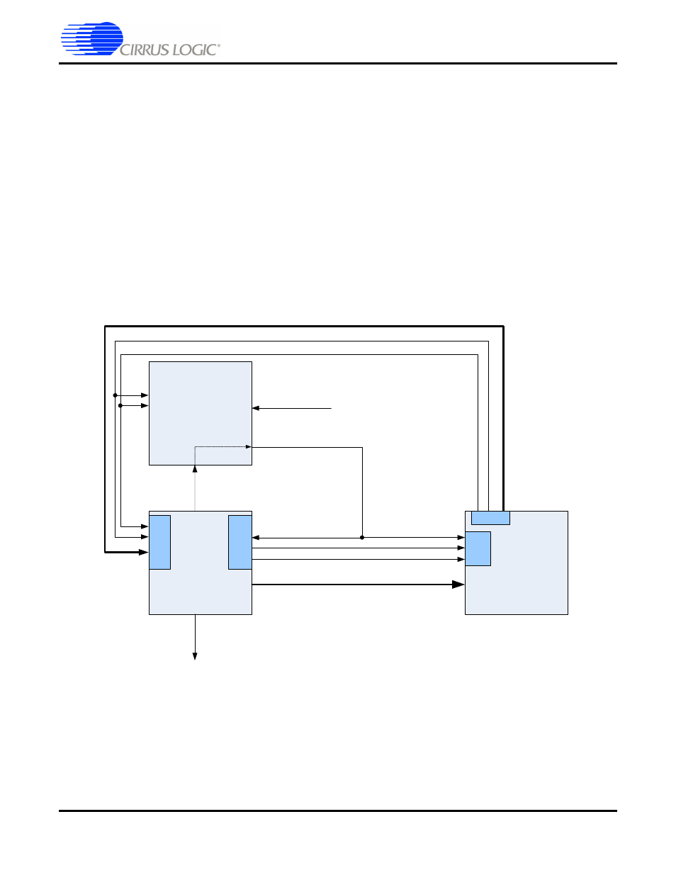
1.3.10.1 Clock and Data Flow for ADC Input
Figure 1-3. ADC Clocking
The ADC clocking architecture is used when the ADCs are used as the only audio input (i.e. S/PDIF is
disabled as described in "
USB (I2S) Audio Input" on page 4-5
), and the audio input source multiplexer
(U1, U2) is used to select on-board audio sources.
illustrates this clocking configuration.
XTAL_OUT from the CS4953xx is MCLK for the system, and the codec masters the input clocks
(MUXED_SCLK/MUXED_LRCLK) of the CS4953xx. The system routing of the clocks was simplified by
using the CS8416 to drive MCLK to the system, but the internal clock multiplexer of the CS8416 is forced
to the OMCK setting to pass XTAL_OUT.
CS4953xx
CS42448
CS8416
MUXED_SCLK
DSP_SCLK
DSP_LRCLK
MUXED_LRCLK
MUXED_DAI[3:0]
XTA
L
_
O
UT
S/PDIF Input
DSP_DA0[3:0]
X
MT
A
S/
PD
IF
O
UT
MUXED_MCLK
DAI
DAO
SDIN
SDOUT