Cs4244, After each input byte is read, and is input to the, Figure 11. timing, i²c write – Cirrus Logic CS4244 User Manual
Page 25: Figure 12. timing, i²c read
DS900F1
25
CS4244
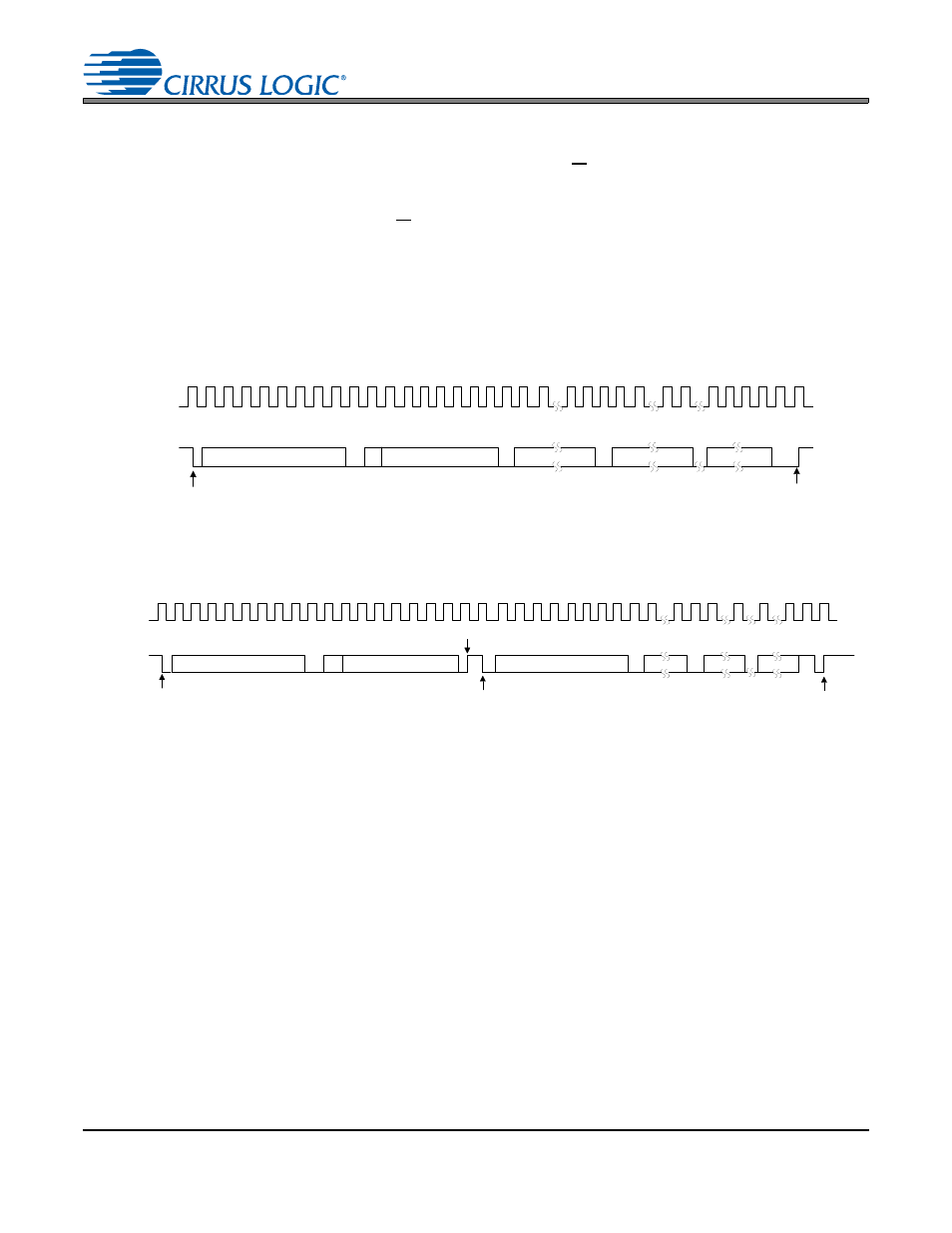
The signal timings for a read and write cycle are shown in
. A Start condition is de-
fined as a falling transition of SDA while the clock is high. A Stop condition is a rising transition while the
clock is high. All other transitions of SDA occur while the clock is low. The first byte sent to the
CS4244
after
a Start condition consists of a 7-bit chip address field and a R/W bit (high for a read, low for a write). The
upper 4 bits of the 7-bit address field are fixed at 0010. To communicate with a
CS4244
, the chip address
field, which is the first byte sent to the
CS4244
, should match 0010 followed by the settings of the ADx pins.
The eighth bit of the address is the R/W bit. If the operation is a write, the next byte is the Memory Address
Pointer (MAP) which selects the register to be read or written. If the operation is a read, the contents of the
register pointed to by the MAP will be output. Setting the auto increment bit in MAP allows successive reads
or writes of consecutive registers. Each byte is separated by an acknowledge bit. The ACK bit is output from
the
CS4244
after each input byte is read, and is input to the
CS4244
from the microcontroller after each trans-
mitted byte.
Since the read operation can not set the MAP, an aborted write operation is used as a preamble. As shown
in
, the write operation is aborted after the acknowledge for the MAP byte by sending a stop con-
dition. The following pseudocode illustrates an aborted write operation followed by a read operation.
Send start condition.
Send 0010xxx0 (chip address & write operation).
Receive acknowledge bit.
Send MAP byte, auto increment off.
Receive acknowledge bit.
Send stop condition, aborting write.
Send start condition.
Send 0010xxx1 (chip address & read operation).
Receive acknowledge bit.
Receive byte, contents of selected register.
Send acknowledge bit.
Send stop condition.
Setting the auto increment bit in the MAP allows successive reads or writes of consecutive registers. Each
byte is separated by an acknowledge bit.
4 5 6 7
24 25
SCL
CHIP ADDRESS (WRITE)
MAP BYTE
DATA
DATA +1
START
ACK
STOP
ACK
ACK
ACK
0 0 1 0 AD2 AD1 AD0 0
SDA
INCR
6 5 4 3 2 1 0
7 6 1 0
7 6 1 0
7 6 1 0
0 1 2 3
8 9
12
16 17 18 19
10 11
13 14 15
27 28
26
DATA +n
Figure 11. Timing, I²C Write
SCL
CHIP ADDRESS (WRITE)
MAP BYTE
DATA
DATA +1
START
ACK
STOP
ACK
ACK
ACK
0 0 1 0 AD2 AD1 AD0 0
SDA
CHIP ADDRESS (READ)
START
INCR
6 5 4 3 2 1 0
7 0
7 0
7 0
NO
16
8 9
12 13 14 15
4 5 6 7
0 1
20 21 22 23 24
26 27 28
2 3
10 11
17 18 19
25
ACK
DATA + n
STOP
0 0 1 0 AD2 AD1 AD0 1
Figure 12. Timing, I²C Read