GE Industrial Solutions LC-LW015-Series User Manual
Options, Features, Applications
Data Sheet
March 27, 2008
LC/LW010- and LC/LW015-Series Power Modules:
18 Vdc to 36 Vdc or 36 Vdc to 75 Vdc Inputs, 10 W and 15 W
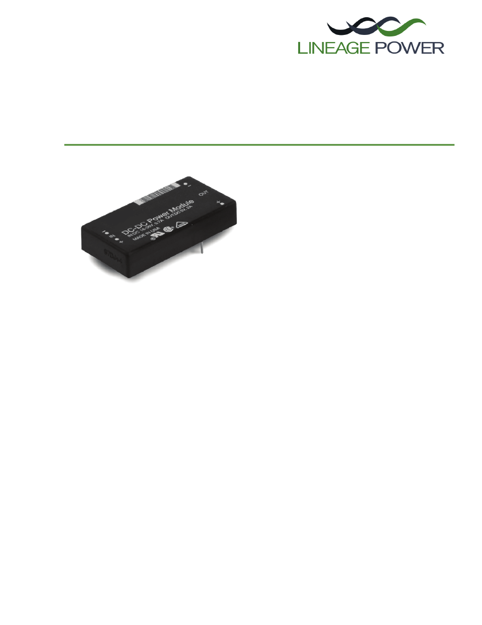
The LC/LW010- and LC/LW015-Series Power Modules use
advanced, surface-mount technology and deliver high-qual-
ity, compact, dc-dc conversion at an economical price.
Options
n
Remote on-off
n
Choice of on/off configuration
n
Short pin: 2.8 mm ± 0.25 mm (0.110 in. ± 0.010 in.)
n
Synchronization (cannot be ordered on units with
remote on/off)
n
Output voltage adjust: 90% to 110% of V
O, nom
(single outputs only)
n
Tight output voltage tolerance
Features
n
Low profile: 10.2 mm x 25.4 mm x 50.8 mm
(0.4 in. x 1.0 in. x 2.0 in.) with standoffs
(9.6 mm (0.38 in.) with standoffs recessed)
n
Wide input voltage range: 18 Vdc to 36 Vdc or
36 Vdc to 75 Vdc
n
Output current limiting, unlimited duration
n
Output overvoltage clamp
n
Undervoltage lockout
n
Input-to-output isolation: 1500 V
n
Operating case temperature range: –40 °C to
+105 °C
n
UL* 1950 Recognized, CSA
†
22.2 No. 950-95
Certified, IEC950, and VDE0805 Licensed
n
CE mark meets 73/23/EEC and 93/68/EEC
directives
‡
n
Within FCC and VDE Class A radiated limits
Applications
n
Telecommunications
n
Distributed power architectures
n
Private branch exchange (PBX)
n
Voice and data multiplexing
Description
The L Single- and Dual-Output-Series Power Modules are low-profile, dc-dc converters that operate over an
input voltage range of 18 Vdc to 36 Vdc or 36 Vdc to 75 Vdc and provide one or two precisely regulated out-
puts. The outputs are isolated from the input, allowing versatile polarity configurations and grounding connec-
tions. The modules have a maximum power rating of 10 W to 15 W and efficiencies of up to 84% for a 5 V
output and 82% for a 3.3 V output. Built-in filtering for both input and output minimizes the need for external fil-
tering.
* UL is a registered trademark of Underwriters Laboratories, Inc.
† CSA is a registered trademark of Canadian Standards Association.
‡ This product is intended for integration into end-use equipment. All the required procedures for CE marking of end-use equipment should be followed. (The CE mark is placed on selected products.)
Document Outline
- Options
- Features
- Applications
- Description
- Absolute Maximum Ratings
- Electrical Specifications
- Characteristic Curves
- Figure 1. LC010 Input Current vs. Input Voltage at IO = IO, max and TC = 25 °C
- Figure 2. LC015 Input Current vs. Input Voltage at IO = IO, max and TC = 25 °C
- Figure 3. LW010 Input Current vs. Input Voltage at IO = IO, max and TC = 25 °C
- Figure 4. LW015 Input Current vs. Input Voltage at IO = IO, max and TC = 25 °C
- Figure 5. Lx010x/Lx015x Single-Output Load Regulation, Normalized Output Voltage vs. Normalized Output Current at TC = 25 °C
- Figure 6. Lx010AJ Typical Load Regulation of Output1 with Fixed IO2 = 0.5 A at TC = 25 °C
- Figure 7. Lx010AJ Typical Cross Regulation, VO1 vs. IO2 with Fixed IO1 = 0.1 A at TC = 25 °C
- Figure 8. Lx010AJ Typical Cross Regulation, VO1 vs. IO2 with Fixed IO1 = 1.0 A at TC = 25 °C
- Figure 9. Lx010BK, CL Load Regulation of Output1 with Fixed IO2 = 0.5 * IO, max at TC = 25 °C, Normalized VO1 vs. Normalized Current IO1
- Figure 10. Lx010BK, CL Typical Cross Regulation, Normalized VO1 vs. Normalized IO2 with Fixed IO1 = IO, min at TC = 25 °C
- Figure 11. Lx010BK, CL Typical Cross Regulation, Normalized VO1 vs. Normalized IO2 with Fixed IO1 = IO, max at TC = 25 °C
- Figure 12. Lx010x/Lx015x Single-Output Normalized Output Current vs. Normalized Output Voltage at TC = 25 °C
- Figure 13. Lx010xx Dual-Output Normalized Output Current vs. Normalized Output Voltage at TC = 25 °C with Other Output at IO, min
- Figure 14. Lx010xx Dual-Output Normalized Output Current vs. Normalized Output Voltage at TC = 25 °C with Other Output at IO = IO, max
- Figure 15. LC015A Typical Efficiency vs. Output Current at TC = 25 °C
- Figure 16. LC015B, C Typical Efficiency vs. Normalized Output Current at TC = 25 °C
- Figure 17. LC010D and LC015D Typical Efficiency vs. Output Current at TC = 25 °C
- Figure 18. LC015F Typical Efficiency vs. Output Current at TC = 25 °C
- Figure 19. LC010A, B, C Typical Efficiency vs. Normalized Output Current at TC = 25 °C
- Figure 20. LC010F Typical Efficiency vs. Output Current at TC = 25 °C
- Figure 21. LC010AJ, BK, CL Typical Efficiency vs. Normalized Output Current at TC = 25 °C
- Figure 22. LW015A Typical Efficiency vs. Output Current at TC = 25 °C
- Figure 23. LW015B, C Typical Efficiency vs. Normalized Output Current at TC = 25 °C
- Figure 24. LW010D, 015D Typical Efficiency vs. Output Current at TC = 25 °C
- Figure 25. LW015F Typical Efficiency vs. Output Current at TC = 25 °C
- Figure 26. LW010A, B, C Typical Efficiency vs. Normalized Output Current at TC = 25 °C
- Figure 27. LW010F Typical Efficiency vs. Output Current at TC = 25 °C
- Figure 28. LW010AJ, BK, CL Typical Efficiency vs. Normalized Output Current at TC = 25 °C
- Figure 29. Single-Output Typical Output Voltage for Step Load Change from 50% to 75% of IO = IO, max
- Figure 30. Single-Output Typical Output Voltage for Step Load Change from 50% to 25% of IO = IO, max
- Figure 31. Typical Output Voltage Start-Up when Input Voltage Is Applied; IO = 80% of IO, max, VI = Nominal Line
- Figure 32. Typical Output Voltage Start-Up when Signal Is applied to Remote On/Off; IO = 80% of IO, max
- Test Configurations
- Figure 33. Input Reflected-Ripple Test Setup
- Figure 34. Peak-to-Peak Output Noise Measurement Test Setup for Single Outputs
- Figure 35. Output Voltage and Efficiency Measurement Test Setup for Single Outputs
- Figure 36. Peak-to-Peak Output Noise Measurement Test Setup for Dual Outputs
- Figure 37. Output Voltage and Efficiency Measurement Test Setup for Dual Outputs
- Design Considerations
- Safety Considerations
- Feature Descriptions
- Thermal Considerations
- Figure 41. LW010 and LC010 Case Temperature Measurement Location
- Figure 42. LW015 and LC015 Case Temperature Measurement Location
- Heat Transfer Characteristics
- Figure 43. LW010/LC010 Forced Convection Power Derating; Either Orientation
- Figure 44. LC015 Forced Convection Power Derating; Either Orientation
- Figure 45. LW015 Forced Convection Power Derating; Either Orientation
- Figure 46. LC015A Power Dissipation at Maximum Case Temperature
- Figure 47. LC015B, C Typical Power Dissipation vs. Normalized Output Current at TC = 25 °C
- Figure 48. LC010D, 015D Typical Power Dissipation vs. Output Current at TC = 25 °C
- Figure 49. LC015F Typical Power Dissipation vs. Output Current at Maximum Case Temperature
- Figure 50. LC010A, B, C Typical Power Dissipation vs. Normalized Output Current at TC = 25 °C
- Figure 51. LC010F Typical Power Dissipation vs. Output Current at TC = 25 °C
- Figure 52. LC010AJ, BK, CL Typical Power Dissipation vs. Normalized Output Current at TC = 25 °C
- Figure 53. LW015A Power Dissipation at Maximum Case Temperature
- Figure 54. LW015B, C Typical Power Dissipation vs. Normalized Output Current at TC = 25 °C
- Figure 55. LW010D, LW015D Typical Power Dissipation vs. Output Current at TC = 25 °C
- Figure 56. LW010D9 Typical Power Dissipation vs. Output Current at TC = 25 °C with Output Voltage Trimmed Up to 2.5 V
- Figure 57. LW015F Power Dissipation at Maximum Case Temperature
- Figure 58. LW010A, B, C Typical Power Dissipation vs. Normalized Output Current at TC = 25 °C
- Figure 59. LW010F Typical Power Dissipation vs. Output Current at TC = 25 °C
- Figure 60. LW010AJ, BK, CL Typical Power Dissipation vs. Normalized Output Current at TC = 25 °C
- Module Derating
- Layout Considerations
- Outline Diagram
- Recommended Hole Pattern
- Ordering Information