Feature specifications, Data sheet, Austin microlynx – GE Industrial Solutions Austin MicroLynx II 12V SIP User Manual
Page 5
Data Sheet
January 18, 2010
Austin MicroLynx
II
TM
12V SIP Non-isolated Power Modules:
8.3 – 14Vdc input; 0.75Vdc to 5.5Vdc Output; 6A output current
LINEAGE
POWER
5
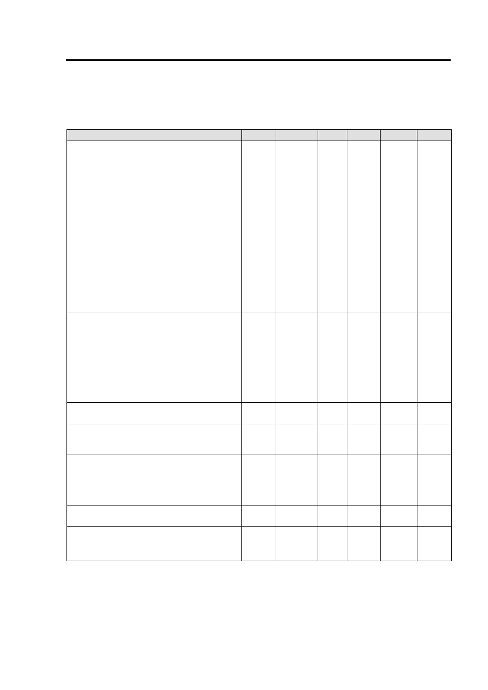
Feature Specifications
Unless otherwise indicated, specifications apply over all operating input voltage, resistive load, and temperature
conditions. See Feature Descriptions for additional information.
Parameter
Device
Symbol
Min
Typ
Max
Unit
On/Off Signal interface
Device code with Suffix “4” – Positive logic
(On/Off is open collector/drain logic input;
Signal referenced to GND - See feature description
section)
Input High Voltage (Module ON)
All
V
IH
―
―
V
IN, max
V
Input High Current
All
I
IH
―
― 10 μA
Input Low Voltage (Module OFF)
All
V
IL
-0.2 ― 0.3 V
Input Low Current
All
I
IL
― 0.2 1 mA
Device Code with no suffix – Negative Logic
(On/OFF pin is open collector/drain logic input with
external pull-up resistor; signal referenced to GND)
Input High Voltage (Module OFF)
All
V
IH
2.5 ―
V
IN,max
Vdc
Input High Current
All
I
IH
0.2
1 mA
Input Low Voltage (Module ON)
All
V
IL
-0.2 ― 0.3 Vdc
Input low Current
All
I
IL
― 10 μA
Turn-On Delay and Rise Times
(I
O
=I
O, max ,
V
IN
= V
IN, nom,
T
A
= 25
o
C, )
Case 1: On/Off input is set to Logic Low (Module
ON) and then input power is applied (delay from
instant at which V
IN
=V
IN, min
until Vo=10% of Vo,set)
All Tdelay ― 3 ― msec
Case 2: Input power is applied for at least one second
and then the On/Off input is set to logic Low (delay from
instant at which Von/Off=0.3V until Vo=10% of Vo, set)
All Tdelay ― 3 ― msec
Output voltage Rise time (time for Vo to rise from 10%
of V
o,set
to 90% of Vo, set)
All Trise
― 4 6 msec
Output voltage overshoot – Startup
―
1
% V
O, set
I
O
= I
O, max
; V
IN
= 8.3 to 14Vdc, T
A
= 25
o
C
Sequencing Delay time
Delay from V
IN, min
to application of voltage on SEQ pin
All
Ts
EQ-delay
10
msec
Tracking Accuracy (Power-Up: 2V/ms)
All
|V
SEQ
–V
o
|
100 200 mV
(Power-Down: 1V/ms)
All
|V
SEQ
–V
o
|
300 500 mV
(V
IN, min
to V
IN, max
; I
O, min
to I
O, max
V
SEQ
< V
o
)
Overtemperature Protection
All T
ref
⎯
140
⎯
°C
(See Thermal Consideration section)
Input Undervoltage Lockout
Turn-on Threshold
All
7.9 V
Turn-off Threshold
All
7.8 V