Pin configuration – Rainbow Electronics ATA6834 User Manual
Page 3
3
9122B–AUTO–10/08
ATA6833/ATA6834 [Preliminary]
2.
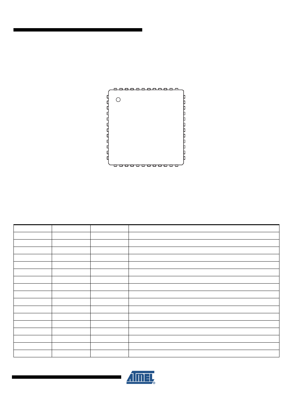
Pin Configuration
Figure 2-1.
Pinning QFN48
Note:
YWW
Date code (Y = Year - above 2000, WW = week number)
ATA683x Product
name
ZZZZZ Wafer
lot
number
AL Assembly
sub-lot
number
RWD
WDD
EN1
NC
NC
GND
NC
CC
WD
/RE
S
ET
VMODE
VINT
Atmel YWW
ATA6
833
/ATA6
83
4
ZZZZZ-AL
CPLO1
CPHI1
CPLO2
CPHI2
CPOUT
S
1
H1
S
2
H2
S3
H
3
DG
3
NC
PBAT
VG
L1
L2
L
3
PGND
VBAT
EN2
VBAT
S
W
NC
VCC
TXD
IH
3
IL2
IH2
RXD
DG1
DG2
IH1
IL1
IL
3
NC
LIN
4
8
47 46 45 44 4
3
42 41 40
3
9
38
3
7
1
3
14 15 16 17 1
8
19 20 21 22 2
3
24
1
2
3
4
5
6
7
8
9
10
11
12
3
6
3
5
3
4
33
3
2
3
1
3
0
29
2
8
27
26
25
Table 2-1.
Pin Description
Pin
Symbol
I/O
Function
1
VMODE
I
Selector for V
CC
and interface logic voltage level
2
VINT
I/O
Blocking capacitor
3
RWD
I
Resistor defining the watchdog interval
4
CC
I/O
RC combination to adjust cross conduction time
5
/RESET
O
Reset signal for microcontroller
6
WD
I
Watchdog trigger signal
7
WDD
I
Enable and disable the watchdog
8
EN1
I
Microcontroller output to switch system in Sleep Mode
9
N.C.
Connect to GND
10
N.C.
Connect to GND
11
GND
I
Ground
12
NC
Connect to GND
13
LIN
I/O
LIN-bus terminal
14
NC
Connect to GND
15
TXD
I
Transmit signal to LIN bus from microcontroller
16
IL3
I
Control Input for output L3
17
IH3
I
Control Input for output H3