Electrical characteristics (continued) – Rainbow Electronics ATA6834 User Manual
Page 21
21
9122B–AUTO–10/08
ATA6833/ATA6834 [Preliminary]
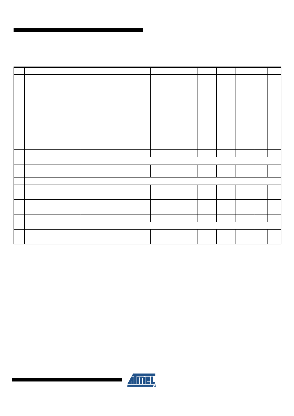
8.21
Propagation delay time,
high-side driver from high
to low
t
HxHL
0.9
µs
A
8.22
Propagation delay time,
high-side driver from low to
high
t
HxLH
0.9
µs
A
8.23 Fall time high-side driver
V
VBAT
= 13.5V,
C
Gx
= 5 nF
t
Hxf
TBD
µs
A
8.24 Rise time high-side driver
V
VBAT
= 13.5V,
C
Gx
= 5 nF
t
Hxr
TBD
µs
A
8.25
Short circuit detection
voltage
V
SC
3.5
4
4.5
V
A
8.26 Short circuit detection time
t
SC
5.4
6
6.6
µs
A
Cross Conduction Timer
8.27
Cross conduction time
constant
K
CC
TBD
0.41
TBD
B
9
Input EN2
9.1 Input low level threshold
V
IL
2.3
3.6
V
A
9.2 Input high level threshold
V
IH
2.8
4.0
V
A
9.3 Hysteresis
HYS
0.47
V
C
9.4 Pull-down resistor
R
PD
50
100
200
k
Ω
A
9.5 Debounce time
t
db
10
20
25
µs
A
10 Diagnostic Outputs DG1, DG2, DG3
10.1 Low level output current
V
DG
= 0.4V
IL
2
mA
A
10.2 High level output current
V
DG
= VCC – 0.4V
IH
–2
mA
A
8.
Electrical Characteristics (Continued)
All parameters given are valid for 5.5V
≤
V
VBAT
≤
18V and for –40°C
≤
T
J
≤
150°C (200°C) unless stated otherwise. All values refer to PIN
GND. [xxx] Values for the ATA6834.
No. Parameters
Test Conditions
Pin
Symbol
Min.
Typ.
Max.
Unit Type*
*) Type means: A = 100% tested, B = 100% correlation tested, C = Characterized on samples, D = Design parameter