10 diagnostic outputs d1 - d3, 11 lin transceiver – Rainbow Electronics ATA6834 User Manual
Page 12
12
9122B–AUTO–10/08
ATA6833/ATA6834 [Preliminary]
3.10
Diagnostic Outputs D1 - D3
As mentioned in the sections above, the diagnostic outputs DG1 to DG3 are used to signal fail-
ures. This is summarized in the following table.
In order to differentiate between LIN and EN2 wake-up, DG1 output will be set to LOW or HIGH
respectively. LOW indicates wake-up by LIN, HIGH indicates wake-up by EN2. DG1 output will
be cleared by the first valid watchdog trigger after wake-up or by the first rising edge at one of
the control inputs (IL1 to IL3 and IH1 toIH3) if the watchdog is disabled.
3.11
LIN Transceiver
ATA6833 and ATA6834 include a fully integrated LIN transceiver complying with LIN specifica-
tion 2.1 and SAEJ2602 2. The transceiver consists of a low-side driver with slew rate control,
wave shaping, current limiting, and a high voltage comparator followed by a debouncing unit in
the receiver.
During transmission, the data applied at pin TXD will be transferred to the bus driver to generate
a bus signal on LIN pin. TXD input has an internal pull-up resistor.
To minimize the electromagnetic emission of the bus line, the bus driver has a built-in slew rate
control and wave-shaping unit. The transmission will be aborted by a thermal shutdown or by a
transition to Sleep Mode.
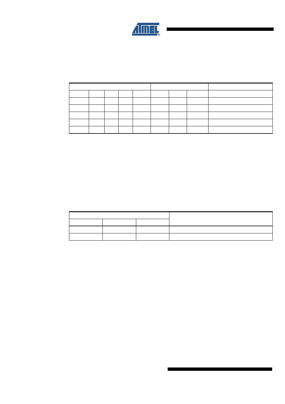
Table 3-2.
Status of the Diagnostic Outputs (Normal Operation)
Device Status
Diagnostic Outputs
Comments
CPOK
OT1
OV
UV
SC
DG1
DG2
DG3
0
X
X
X
X
–
1
–
Charge pump failure
X
1
X
X
X
–
–
1
Overtemperature prewarning
X
X
1
X
X
–
1
–
Overvoltage
X
X
X
1
X
–
1
–
Undervoltage
X
X
X
X
1
1
–
–
Short circuit
Note:
X represents: no effect)
OT1: overtemperature warning
OV: overvoltage of PBAT
UV: undervoltage of PBAT
SC: short circuit
CPOK: charge pump OK
Table 3-3.
Indicating Wake-up Source
Diagnostic Outputs
Wake-up Source
DG1
DG2
DG3
1
–
–
EN2
0
–
–
LIN