Rainbow Electronics ATA6834 User Manual
Page 13
13
9122B–AUTO–10/08
ATA6833/ATA6834 [Preliminary]
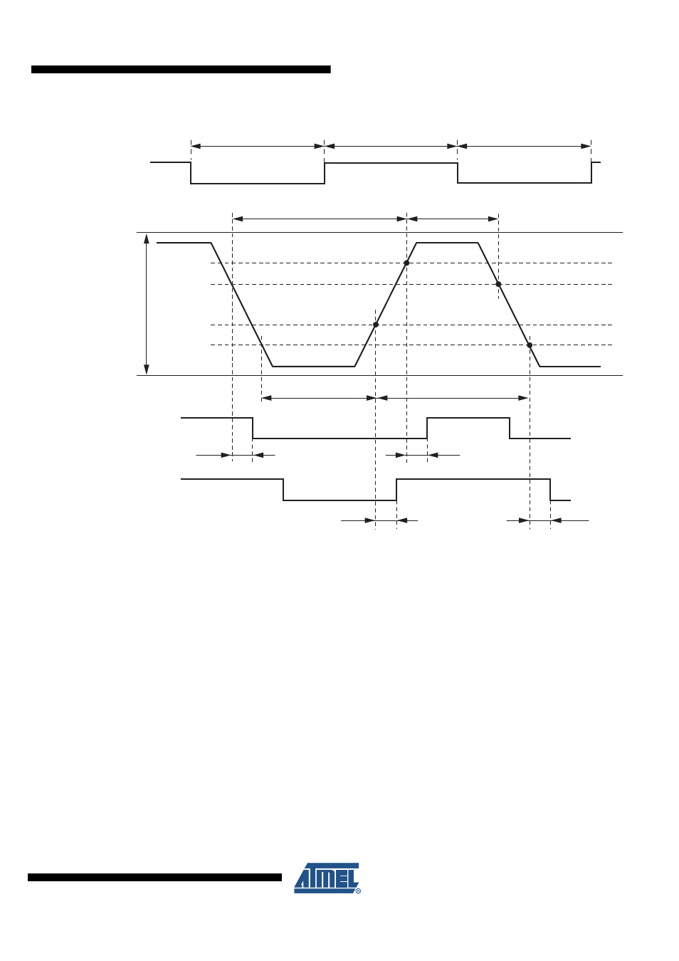
Figure 3-7.
Definition of Bus Timing Parameters
The recessive BUS level is generated from the integrated 30 k
Ω
pull-up resistor in series with an
active diode. This diode protects against reverse currents on the bus line in case of a voltage dif-
ference between the bus line and VSUP (V
BUS
> V
SUP
). No additional termination resistor is
necessary to use the IC as a LIN slave. If this IC is used as a LIN master, the LIN pin is termi-
nated by an external 1 k
Ω
resistor in series with a diode to VBAT.
As PWM communication directly over the LIN transceiver in both directions is possible, there is
no TXD timeout feature implemented in the LIN transceiver.
TXD
(Input to transmitting node)
VS
(Transceiver supply
of transmitting node)
RXD
(Output of receiving node1)
RXD
(Output of receiving node2)
LIN Bus Signal
Thresholds of
receiving node1
Thresholds of
receiving node2
t
Bus_rec(max)
t
rx_pdr(1)
t
rx_pdf(2)
t
rx_pdr(2)
t
rx_pdf(1)
t
Bus_dom(min)
t
Bus_dom(max)
TH
Rec(max)
TH
Dom(max)
TH
Rec(min)
TH
Dom(min)
t
Bus_rec(min)
t
Bit
t
Bit
t
Bit