Converter electrical characteristics – Rainbow Electronics ADC08D1000 User Manual
Page 9
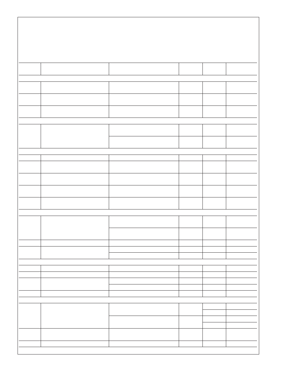
Converter Electrical Characteristics
(Continued)
[Note: This product is currently in development. As such, the parameters specified in this section are DESIGN TAR-
GETS. The specifications in this section cannot be guaranteed until device characterization has taken place.]
The following specifications apply after calibration for V
A
= V
DR
= +1.9V
DC
, OutV = 1.9V, V
IN
FSR (a.c. coupled) = differential
860mV
P-P
, C
L
= 10 pF, Differential, a.c. coupled Sinewave Input Clock, f
CLK
= 1 GHz at 0.5V
P-P
with 50% duty cycle, Non-
Extended Control Mode, R
EXT
= 3300
Ω
±
0.1%, Analog Signal Source Impedance = 100
Ω. Boldface limits apply for T
A
=
T
MIN
to T
MAX
. All other limits T
A
= 25˚C, unless otherwise noted. (Notes 6, 7)
Symbol
Parameter
Conditions
Typical
Limits
Units
(Limits)
ANALOG OUTPUT CHARACTERISTICS
V
BG
Bandgap Reference Output
Voltage
I
BG
=
±
100 µA
1.26
1.22
1.33
V (min)
V (max)
TC V
BG
Bandgap Reference Voltage
Temperature Coefficient
T
A
= −40˚C to +85˚C,
I
BG
=
±
100 µA
28
ppm/˚C
C
LOAD
V
BG
Maximum Bandgap Reference load
Capacitance
80
pF
TEMPERATURE DIODE CHARACTERISTICS
Temperature Diode Voltage
∆I
DIODE
, 100 µA vs. 10 µA,
T
J
= 25˚C
TBD
mV
∆I
DIODE
, 100 µA vs. 10 µA,
T
J
= 85˚C
TBD
mV
CHANNEL-TO-CHANNEL CHARACTERISTICS
Offset Match
2
TBD
LSB (max)
Positive Full-Scale Match
Zero offset selected in Control
Register
6
TBD
mV (max)
Negative Full-Scale Match
Zero offset selected in Control
Register
6
TBD
mV (max)
X-TALK
Crosstalk from I to Q Channel
Aggressor =867 MHz F.S.
Victim = 100 MHz F.S.
-77
dB
X-TALK
Crosstalk from Q to I Channel
Aggressor =867 MHz F.S.
Victim = 100 MHz F.S.
-77
dB
CLOCK INPUT CHARACTERISTICS
V
ID
Differential Clock Input Level
Sine Wave Clock
0.6
0.4
2.0
V
P-P
(min)
V
P-P
(max)
Square Wave Clock
0.6
0.4
2.0
V
P-P
(min)
V
P-P
(max)
I
I
Input Current
V
IN
= 0 or V
IN
= V
A
±
1
µA
C
IN
Input Capacitance (Note 11)
Differential
0.02
pF
Each input to ground
1.5
pF
DIGITAL CONTROL PIN CHARACTERISTICS
V
IH
Logic High Input Voltage
1.4
V (min)
V
IL
Logic Low Input Voltage
0.5
V (max)
I
I
Input Current
V
IN
= 0 or V
IN
= V
A
, Pins 4, 14, 127
±
80
µA
V
IN
= 0 or V
IN
= V
A
, All Other Pins
±
1
µA
C
IN
Input Capacitance (Note 11)
Each input to ground
1.2
pF
DIGITAL OUTPUT CHARACTERISTICS
V
OD
LVDS Differential Output Voltage
OutV = V
A
, measured differentially
600
400
mV
P-P
(min)
900
mV
P-P
(max)
OutV = GND, measured
differentially
450
280
mV
P-P
(min)
680
mV
P-P
(max)
∆ V
O DIFF
Change in LVDS Output Swing
Between Logic Levels
±
1
mV
V
OS
Output Offset Voltage
800
mV
ADC08D1000
www.national.com
9