Figure 11. differential input drive, 1 handling single-ended input signals, Table 5 – Rainbow Electronics ADC08D1000 User Manual
Page 25: 0 applications information
2.0 Applications Information
(Continued)
reduced to 75% of the values indicated. In the Enhanced
Control Mode, these values will be determined by the full
scale range and offset settings in the Control Registers.
TABLE 5. DIFFERENTIAL INPUT TO OUTPUT
RELATIONSHIP (Non-Extended Control Mode, FSR
High)
V
IN
+
V
IN
−
Output Code
V
CM
− 430 mV
V
CM
+ 430 mV
0000 0000
V
CM
− 214 mV
V
CM
+ 214 mV
0100 0000
V
CM
V
CM
0111 1111 /
1000 0000
V
CM
+ 216 mV
V
CM
−216 mV
1100 0000
V
CM
+ 430mV
V
CM
− 430 mV
1111 1111
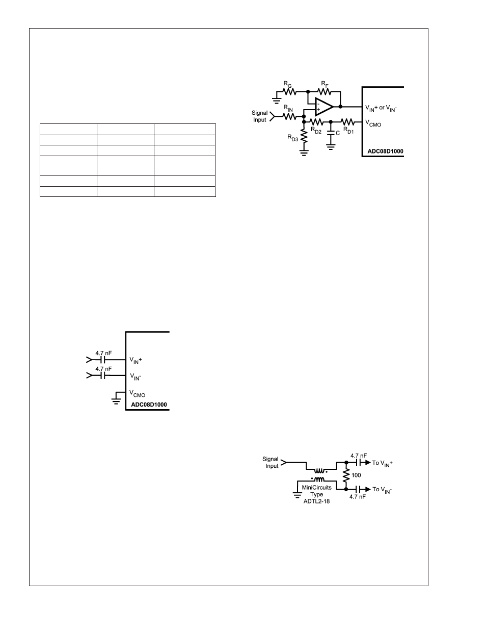
The buffered analog inputs simplify the task of driving these
inputs and the RC pole that is generally used at sampling
ADC inputs is not required. If it is desired to use an amplifier
circuit before the ADC, use care in choosing an amplifier with
adequate noise and distortion performance and adequate
gain at the frequencies used for the application.
Note that a precise d.c. common mode voltage must be
present at the ADC inputs. This common mode voltage,
V
CMO
, is provided on-chip when a.c. input coupling is used
and the input signal is a.c. coupled to the ADC.
When the inputs are a.c. coupled, the V
CMO
output must be
grounded, as shown in Figure 11. This causes the on-chip
V
CMO
voltage to be connected to the inputs through on-chip
50k-Ohm resistors.
When the d.c. coupled mode is used, a common mode
voltage must be provided at the differential inputs. This
common mode voltage should track the V
CMO
output pin.
Note that the V
CMO
output potential will change with tem-
perature. The common mode output of the driving device
should track this change.
Full-scale distortion performance falls off rapidly as the
input common mode voltage deviates from V
CMO
. This is
a direct result of using a very low supply voltage to
minimize power. Keep the input common voltage within
50 mV of V
CMO
.
Performance is as good in the d.c. coupled mode as it is
in the a.c. coupled mode, provided the input common
mode voltage at both analog inputs remain within 50 mV
of V
CMO
.
If d.c. coupling is used, it is best to servo the input common
mode voltage, using the V
CMO
pin, to maintain optimum
performance. An example of this type of circuit is shown in
Figure 12.
One such circuit should be used in front of the V
IN
+ input and
another in front of the V
IN
− input. In that figure, R
D1
, R
D2
and
R
D3
are used to divide the V
CMO
potential so that, after being
gained up by the amplifier, the input common mode voltage
is equal to V
CMO
from the ADC. R
D1
and R
D2
are split to
allow the bypass capacitor to isolate the input signal from
V
CMO
. R
IN
, R
D2
and R
D3
will divide the input signal, if nec-
essary. If there is no need to divide the input signal, R
IN
is not
needed. Capacitor "C" in Figure 12 should be chosen to
keep any component of the input signal from affecting V
CMO
.
Be sure that the current drawn from the V
CMO
output does
not exceed 100 µA.
The Input impedance in the d.c. coupled mode (V
CMO
pin not
grounded) consists of a precision 100
Ω resistor between
V
IN
+ and V
IN
− and a capacitance from each of these inputs
to ground. In the a.c. coupled mode the input appears the
same except there is also a resistor of 50K between each
analog input pin and the V
CMO
potential.
Driving the inputs beyond full scale will result in a saturation
or clipping of the reconstructed output.
2.2.1 Handling Single-Ended Input Signals
There is no provision for the ADC08D1000 to adequately
process single-ended input signals. The best way to handle
single-ended signals is to convert them to differential signals
before presenting them to the ADC. The easiest way to
accomplish single-ended to differential signal conversion is
with an appropriate balun-connected transformer, as shown
in Figure 13.
20097444
FIGURE 11. Differential Input Drive
20097455
FIGURE 12. Example of Servoing the Analog Input with
V
CMO
20097443
FIGURE 13. Single-Ended to Differential signal
conversion with a balun-connected transformer
ADC08D1000
www.national.com
25