Des fine adjust, 1 note regarding extended mode offset correction, Figure 10. extended mode offset behaviour – Rainbow Electronics ADC08D1000 User Manual
Page 24: 5 multiple adc synchronization, 0 applications information, 1 the reference voltage, 2 the analog input, 0 functional description
1.0 Functional Description
(Continued)
DES Fine Adjust
Addr: Fh (1111b)
W only (0x007F)
D15
D14
D13
D12
D11
D10
D9
D8
(MSB)
FAM
D7
D6
D5
D4
D3
D2
D1
D0
(LSB)
1
1
1
1
1
1
1
Bits 15:7
Fine Adjust Magnitude. Each code value in
this field delays either the "I" channel or the
"Q" channel sample clock (as determined by
the ADS bit of the DES Coarse Adjust
Register) by approximately 0.1 ps. A value of
00h in this field causes zero adjustment.
Note that the amount of adjustment achieved
with each code will vary with the device
conditions as well as with the Coarse
Adjustment value chosen.
POR State: 0000 0000 b
Bit 6:0
Must be set to 1b
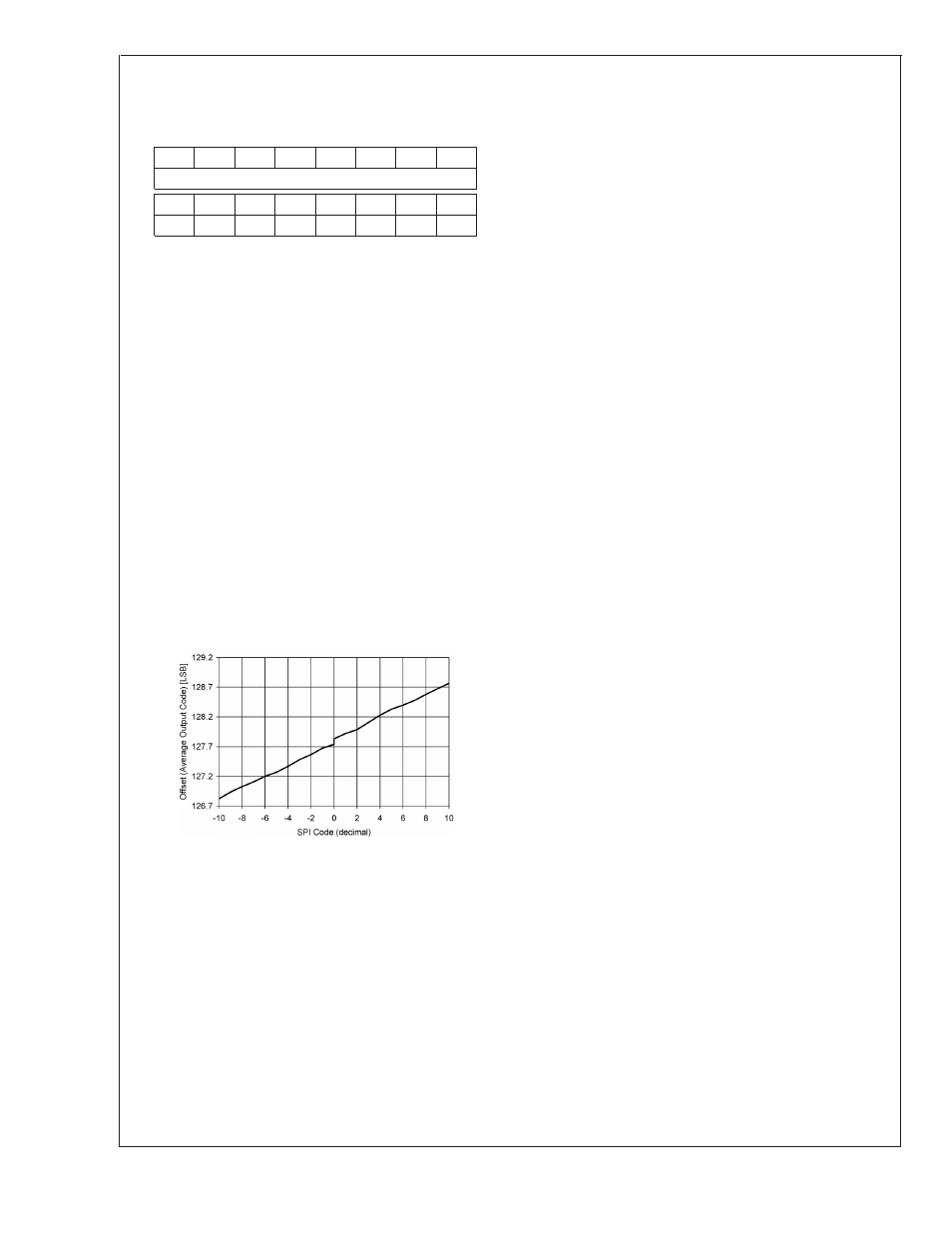
1.4.1 Note Regarding Extended Mode Offset Correction
When using the I or Q channel Offset Adjust registers, the
following information should be noted.
For offest values of +0000 0000 and -0000 0000, the actual
offset is not the same. By changing only the sign bit in this
case, an offset step in the digital output code of about 1/10th
of an LSB is experienced. This is shown more clearly in the
Figure below.
1.5 MULTIPLE ADC SYNCHRONIZATION
The ADC08D1000 has the capability to precisely reset its
sampling clock input to DCLK output relationship as deter-
mined by the user-supplied DCLK_RST pulse. This allows
multiple ADCs in a system to have their DCLK (and data)
outputs transition at the same time with respect to the shared
CLK input that they all use for sampling.
The DCLK_RST signal must observe some timing require-
ments that are shown in Figure 6, Figure 7 and Figure 8 of
the Timing Diagrams. The DCLK_RST pulse must be of a
minimum width and its deassertion edge must observe setup
and hold times with respect to the CLK input rising edge.
These times are specified in the AC Electrical Characteris-
tics Table.
The DCLK_RST signal can be asserted asynchronous to the
input clock. If DCLK_RST is asserted, the DCLK output is
immediately held in a designated state. The state in which
DCLK is held during the reset period is determined by the
mode of operation (SDR/DDR) and the setting of the Output
Edge configuration pin or bit. (Refer to Figure 6, Figure 7 and
Figure 8 for the DCLK reset state conditions). Therefore,
depending upon when the DCLK_RST signal is asserted,
there may be a narrow pulse on the DCLK line during this
reset event. When the DCLK_RST signal is deasserted in
synchronization with the CLK rising edge, the next CLK
falling edge synchronizes the DCLK output with those of
other ADC08D1000s in the system. The DCLK output is
enabled again after a constant delay (relative to the input
clock frequency) which is equal to the CLK input to DCLK
output delay (t
SD
). The device always exhibits this delay
characteristic in normal operation.
The DCLK-RST pin should NOT be brought high while the
calibration process is running (while CalRun is high). Doing
so could cause a digital glitch in the digital circuitry, resulting
in corruption and invalidation of the calibration.
2.0 Applications Information
2.1 THE REFERENCE VOLTAGE
The voltage reference for the ADC08D1000 is derived from a
1.254V bandgap reference, a buffered version of which is
made available at pin 31, V
BG
for user convenience and has
an output current capability of
±
100 µA. This reference
voltage should be buffered if more current is required.
The internal bandgap-derived reference voltage has a nomi-
nal value of 650 mV or 860 mV, as determined by the FSR
pin and described in Section 1.1.4.
There is no provision for the use of an external reference
voltage, but the full-scale input voltage can be adjusted
through a Configuration Register in the Extended Control
mode, as explained in Section 1.2.
Differential input signals up to the chosen full-scale level will
be digitized to 8 bits. Signal excursions beyond the full-scale
range will be clipped at the output. These large signal excur-
sions will also activate the OR output for the time that the
signal is out of range. See Section 2.2.2.
One extra feature of the VBG pin is that it can be used to
raise the common mode voltage level of the LVDS outputs.
The output offset voltage (V
OS
) is typically 800mV when the
VBG pin is used as an output or left unconnected. To raise
the LVDS offset voltage to a typical value of 1050mV the
VBG pin can be connected directly to the supply rails.
2.2 THE ANALOG INPUT
The analog input is a differential one to which the signal
source may be a.c. coupled or d.c. coupled. The full-scale
input range is selected with the FSR pin to be 650 mV
P-P
or
860 mV
P-P
, or can be adjusted to values between 560 mV
P-P
and 840 mV
P-P
in the Extended Control mode through the
Serial Interface. For best performance, it is recommended
that the full-scale range be kept between 595 mV
P-P
and 805
mV
P-P
.
Table 5 gives the input to output relationship with the FSR
pin high and the normal (non-extended) mode is used. With
the FSR pin grounded, the millivolt values in Table 5 are
20097430
FIGURE 10. Extended Mode Offset Behaviour
ADC08D1000
www.national.com
24